Silicon crystal bar cutting processing device

A technology for cutting and processing silicon ingots, which is applied to fine working devices, stone processing equipment, working accessories, etc., can solve the problems of silicon chip recycling, waste of silicon material, poor cutting effect, etc., to achieve convenient recycling, sufficient Utilize water resources, stable cutting effect

Inactive Publication Date: 2021-12-10
张永田
View PDF0 Cites 0 Cited by
  • Summary
  • Abstract
  • Description
  • Claims
  • Application Information

AI Technical Summary

Problems solved by technology

[0003] The traditional silicon ingot cutting device does not cut the silicon ingot evenly, and the silicon debris generated after cutting is not recycled, resulting in a waste of silicon material. At the same time, the silicon ingot is not cut during cutting. It is stable and fixed, the cutting effect is poor, and the surface of the wafer after cutting is dirty. In order to solve the above problems, a silicon crystal ingot cutting processing device is proposed in this application.

Method used


Image

  • Silicon crystal bar cutting processing device
  • Silicon crystal bar cutting processing device
  • Silicon crystal bar cutting processing device

Examples


Embodiment Construction

[0025] In order to make the object, technical solution and advantages of the present invention clearer, the present invention will be further described in detail below in combination with specific embodiments and with reference to the accompanying drawings.

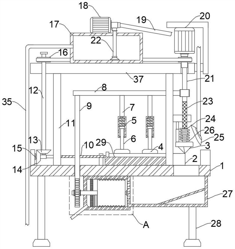
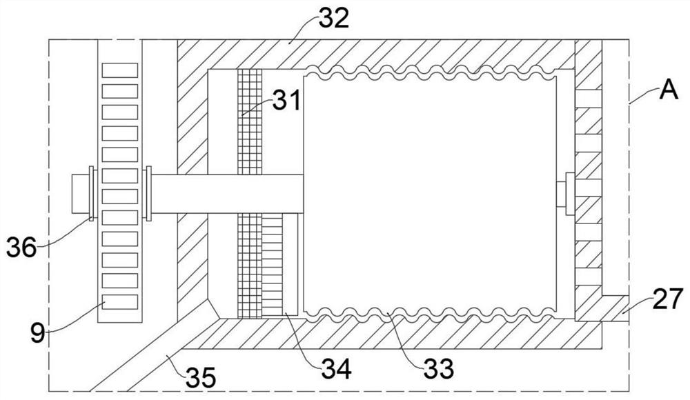
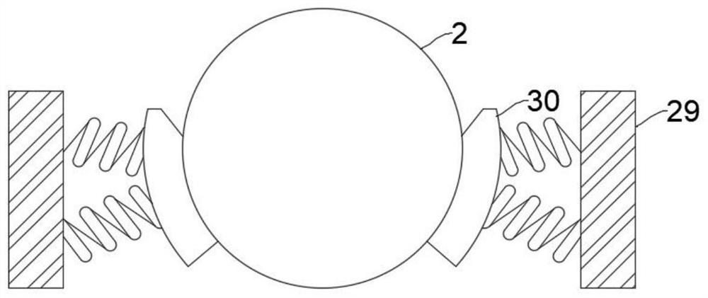
[0026] Such as figure 1 , figure 2 , image 3 , Figure 4 As shown, a silicon ingot cutting and processing device proposed by the present invention includes a platform 1, one end of the platform 1 is provided with a discharge chute, two support columns 11 are fixed on the upper end of the platform 1, and the upper ends of the two support columns 11 are fixed together Connected with a top plate 37, the upper end of the platform 1 is fixedly connected with two baffles 29, and the opposite ends of the two baffles 29 are fixedly connected with a first spring, and the two first springs are fixedly connected with an arc-shaped plate 30, two The inner wall of the curved plate 30 is slidably connected with the silicon crystal...


PUM


Abstract

The invention belongs to the technical field of semiconductors, and particularly relates to a silicon crystal bar cutting processing device which comprises a platform. A discharging groove is formed in one end of the platform, two supporting columns are fixed to the upper end of the platform, the upper ends of the two supporting columns are jointly and fixedly connected with a top plate, the upper end of the platform is fixedly connected with two baffles, the opposite ends of the two baffles are fixedly connected with first springs, the two first springs are fixedly connected with arc-shaped plates, a first telescopic rod is fixedly connected with a lead screw, the upper end of the platform is fixedly connected with a limiting block, the lead screw is in threaded connection with the limiting block, the lead screw is fixedly connected with an abutting block, and the abutting block abuts against one end of a silicon crystal bar. According to the silicon crystal bar cutting processing device provided by the invention, silicon crystal bars are cut at equal intervals, cutting is stable, meanwhile, chippings obtained after cutting can be smashed and recycled, and water resources can be saved while wafers are cleaned and cooled.

Description

technical field [0001] The invention relates to the technical field of semiconductors, in particular to a silicon crystal rod cutting and processing device. Background technique [0002] Silicon wafers are purified from silicon elements, and then these pure silicon are made into long silicon crystal rods, which become the material of quartz semiconductors for manufacturing integrated circuits. After photolithography, grinding, polishing, slicing and other procedures, polycrystalline silicon is melted and pulled out Crystalline silicon ingots are then sliced ​​into thin wafers. [0003] The traditional silicon ingot cutting device does not cut the silicon ingot evenly, and the silicon debris generated after cutting is not recycled, resulting in a waste of silicon material. At the same time, the silicon ingot is not cut during cutting. Stable and fixed, poor cutting effect, dirty wafer surface after cutting, etc. In order to solve the above problems, a silicon crystal ingot c...

Claims


Application Information

Patent Timeline
IPC IPC(8): B28D5/04B28D7/00B28D7/02B02C4/20
CPCB28D5/04B28D5/0058B28D5/0076B02C4/20
Inventor 张永田
Owner 张永田
Why Eureka
Try Eureka