Preparation method of flash memory device

A flash memory device and trench technology, applied in the field of flash memory device manufacturing, can solve problems such as mis-grinding of a silicon oxide layer, and achieve the effects of improving uniformity, improving reliability, and simplifying manufacturing processes

Pending Publication Date: 2021-12-10
SHANGHAI HUALI INTEGRATED CIRCUTE MFG CO LTD
View PDF4 Cites 0 Cited by
  • Summary
  • Abstract
  • Description
  • Claims
  • Application Information

AI Technical Summary

Problems solved by technology

[0004] The purpose of the present invention is to provide a method for preparing a flash memory device, so as to solve the problem that the silicon oxide layer around the top of the groove where the tungsten source line is deposited is easily misground when preparing the tungsten source line of the flash memory device

Method used


Image

  • Preparation method of flash memory device
  • Preparation method of flash memory device
  • Preparation method of flash memory device

Examples


Embodiment Construction

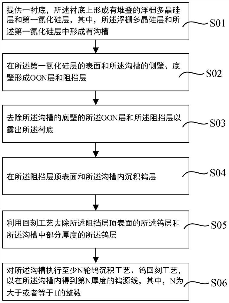
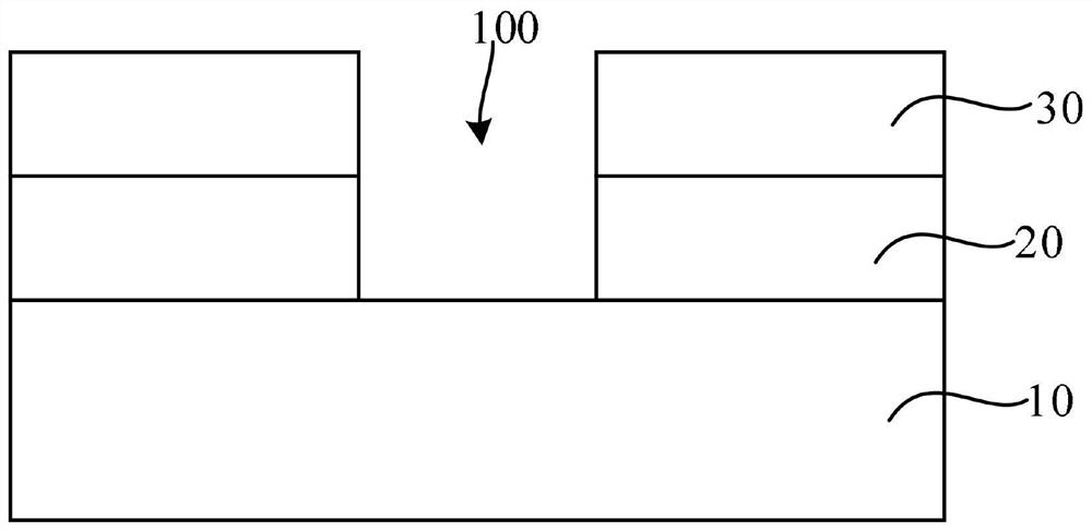
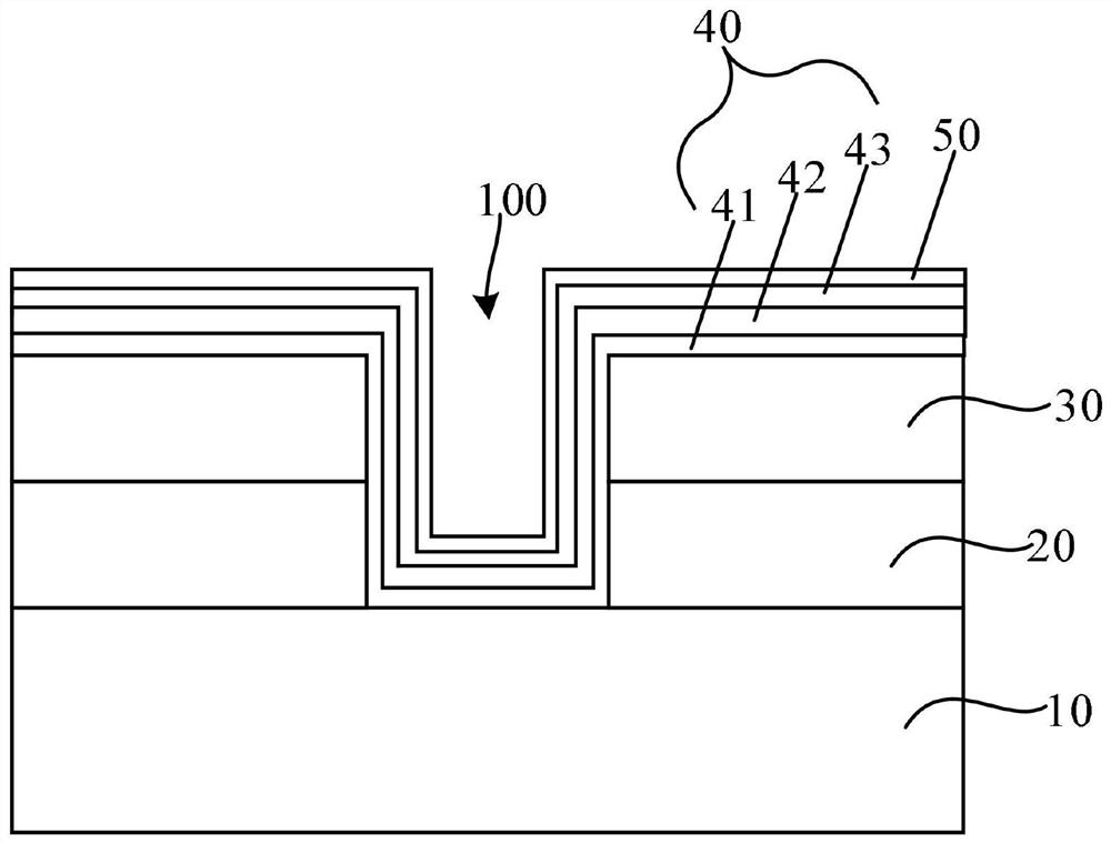
[0036] The preparation method of the flash memory device proposed by the present invention will be further described in detail below in conjunction with the accompanying drawings and specific embodiments. The advantages and features of the present invention will become clearer from the following description. It should be noted that all the drawings are in a very simplified form and use imprecise scales, and are only used to facilitate and clearly assist the purpose of illustrating the embodiments of the present invention. In addition, the structures shown in the drawings are often a part of the actual structure. In particular, each drawing needs to display different emphases, and sometimes uses different scales.

[0037] In the early stage of the experiment, the inventor tried to solve the problem that the silicon oxide layer around the top of the trench where the tungsten source line was deposited was easily misgrinded. After the tungsten metal deposition process and before ...


PUM


Abstract

The invention provides a preparation method of a flash memory device. The preparation method comprises the following steps: providing a substrate, a floating gate polycrystalline silicon layer and a first silicon nitride layer which are stacked, and forming a groove on the substrate; forming an OON layer and a barrier layer; depositing a tungsten layer in the groove; performing an etching-back process on the tungsten layer; and executing at least N rounds of tungsten deposition process and tungsten back etching process so as to obtain a tungsten source line with the Nth thickness in the groove, wherein N is an integer greater than or equal to 1. The traditional CMP process does not need to be executed between the first deposition process and the first back etching process, and at least N turns of tungsten deposition process and tungsten back etching process are continuously executed for the groove after the first back etching process to obtain the final tungsten source line. The situation that the second silicon oxide layer in the OON layer on the first silicon nitride layer around the groove is removed by mistake through grinding due to the CMP technology is avoided, and meanwhile the uniformity of the thickness of the tungsten source line in the groove is improved.

Description

technical field [0001] The invention relates to the technical field of flash memory device manufacturing, in particular to a preparation method of a flash memory device. Background technique [0002] In the current semiconductor industry, Super Flash (Super Flash) technology, as a mainstream storage technology, has developed rapidly in recent years. High, ultra-fast access speed and easy to erase and many other advantages, so it has been widely used in many fields such as microcomputers and automatic control. [0003] In Super Flash, its source line structure generally includes a substrate, a floating gate polysilicon layer, a silicon nitride layer, and a silicon oxide layer, wherein the floating gate polysilicon layer, silicon nitride layer, and silicon oxide layer are formed with trenches, OON sidewalls and barrier layers are formed on the sidewalls of the trenches. When preparing the tungsten source line, tungsten metal is first deposited in the trench, and then the sur...

Claims


Application Information

Patent Timeline
Patent Type & Authority Applications(China)
IPC IPC(8): H01L21/768H01L23/48
CPCH01L21/76847H01L21/76877H01L23/481
Inventor 李荷芸曹坚张亮
Owner SHANGHAI HUALI INTEGRATED CIRCUTE MFG CO LTD
Why Eureka
Try Eureka