Gallium nitride power device with low saturation current characteristic

A technology of saturation current and power devices, which is applied in the direction of electrical components, semiconductor devices, circuits, etc., can solve the problem of large saturation current of gallium nitride power devices, etc., and achieve the effect of improving short-circuit resistance

Pending Publication Date: 2021-12-10
SOUTHEAST UNIV +1
View PDF3 Cites 0 Cited by
  • Summary
  • Abstract
  • Description
  • Claims
  • Application Information

AI Technical Summary

Problems solved by technology

[0005] Aiming at the problem of large saturation current of GaN power devices, the present invention proposes a novel structure of GaN power devices, which effectively reduces the saturation

Method used


Image

  • Gallium nitride power device with low saturation current characteristic
  • Gallium nitride power device with low saturation current characteristic
  • Gallium nitride power device with low saturation current characteristic

Examples


Example Embodiment

[0021] The present invention will be described in detail below with reference to the drawings:

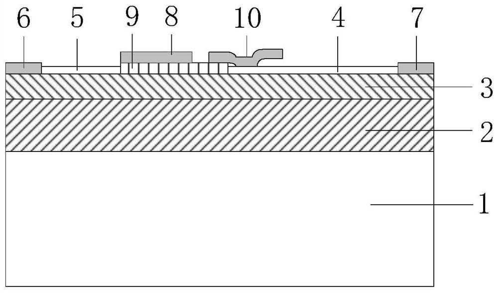
[0022] The gallium nitride power device having a low saturation current characteristic of the present invention includes: a gallium nitride buffer layer 2 above the p-type silicon substrate 1, and the gallium nitride buffer layer 2 is provided above the p-type silicon substrate 1. There is a metal gallium nitrogen barrier layer 3, and the aluminum gallium nitrogen barrier layer 3 is provided as a source 6 and a drain 7 as the source 6 and the drain, respectively, and the input \ output of both ends of the aluminum gallium barrier layer 3 to the periphery. The source 6 metal forms ohmic contact with the left end of the aluminum gallium nitrogen barrier layer 3, the drain 7 metal and the aluminum gallium nitrogen barrier layer 3 form ohmic contact, and the aluminum gallium nitrogen barrier layer 3 is provided with a p-type gallium nitride layer. 9. Plant the p-type gallium nitride layer ...


PUM


Abstract

The invention relates to a gallium nitride power device with a low saturation current characteristic. The device is characterized in that a gallium nitride buffer layer, an aluminum-gallium-nitrogen barrier layer, a source electrode and a drain electrode are arranged above a P-type silicon substrate and are used as input and output for connecting two ends of the aluminum-gallium-nitrogen barrier layer to the periphery, and the source electrode and the left end of the aluminum-gallium-nitrogen barrier layer form ohmic contact; the drain electrode metal and the right end of the aluminum-gallium-nitrogen barrier layer form ohmic contact, a P-type gallium nitride layer is arranged above the aluminum-gallium-nitrogen barrier layer, gate electrode metal is arranged above the P-type gallium nitride layer to connect the aluminum-gallium-nitrogen barrier layer to input and output at the periphery of the structure, and the gate electrode metal and the P-type gallium nitride layer form Schottky contact; and the P-type gallium nitride layer and the grid electrode are close to the source electrode and far away from the drain electrode between the source electrode and the drain electrode, and a nitride passivation layer is arranged between the drain electrode above the aluminum gallium nitrogen barrier layer and the P-type gallium nitride. The structure of the gallium nitride power device can effectively reduce saturation current of the gallium nitride power device, and safety and reliability of the whole device structure are improved.

Description

technical field [0001] The invention mainly relates to the technical field of power integrated circuits, specifically, it is especially suitable for many power control and processing fields such as switching power supplies, motor control, automotive electronic systems, and household appliances. Background technique [0002] Today's semiconductor industry has increasing requirements for power devices, mainly including high power density, low on-resistance, high reliability, high frequency, small size and strong radiation resistance. However, the performance of silicon-based power devices, mainly metal-oxide-semiconductor field-effect transistors and insulated-gate bipolar transistors, has approached the theoretical limit of their materials and cannot meet the higher requirements for power devices in the next generation of power electronic systems. The "silicon limit" is critical. GaN material is one of the representatives of wide bandgap semiconductor materials. In the past ...

Claims


Application Information

Patent Timeline
IPC IPC(8): H01L29/778H01L29/06H01L29/40
CPCH01L29/7781H01L29/0607H01L29/0692H01L29/402
Inventor 张龙崔永久马杰骆敏刘培港王肖娜孙伟锋时龙兴
Owner SOUTHEAST UNIV
Why Eureka
Try Eureka