Light-emitting semiconductor and its preparation method

A technology of light-emitting semiconductors and light-emitting structures, applied in semiconductor devices, electrical components, circuits, etc., can solve problems affecting brightness extraction, electrode conduction effects, film cracks, etc., and achieve the effect of avoiding fracture and aggregation

Active Publication Date: 2022-02-11
HGC (WUHAN) TECH CO LTD
View PDF0 Cites 0 Cited by
  • Summary
  • Abstract
  • Description
  • Claims
  • Application Information

AI Technical Summary

Problems solved by technology

[0003] In the prior art, the LED chip introduces an omnidirectional reflective structure to improve the brightness of the chip. However, the characteristic of Ag is that it is easy to agglomerate, causing the Ag reflective layer to easily gather metal at the edge of the photoresist, resulting in the incomplete reflective layer. The upper layer is coated sequentially, and cracks in the film layer will appear, and the electrodes will be turned on; at present, an edge inclined space area is formed on the surface of the insulating layer near the reflective layer by corroding the insulating layer, and the edge of the Ag reflective layer is covered on the inclined surface. To reduce the degree of metal accumulation
Since the thickness of the insulating layer will affect the extraction of brightness, the above method will thin the insulating layer during the etching process, which will affect the extraction of brightness; if the brightness after thinning is maintained, the overall thickness of the insulating layer needs to be increased. thicker, the deeper the depth of the through hole on the insulating layer, the subsequent deposition of metal on the insulating layer will affect the coverage of the metal at the through hole, resulting in a metal fault covered by the side wall of the through hole, which will affect the conduction of the electrode

Method used


Image

  • Light-emitting semiconductor and its preparation method
  • Light-emitting semiconductor and its preparation method
  • Light-emitting semiconductor and its preparation method

Examples


Embodiment Construction

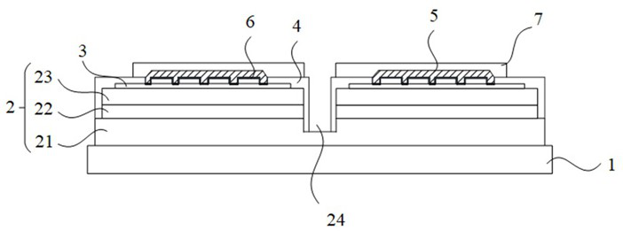
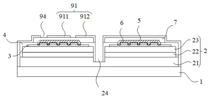
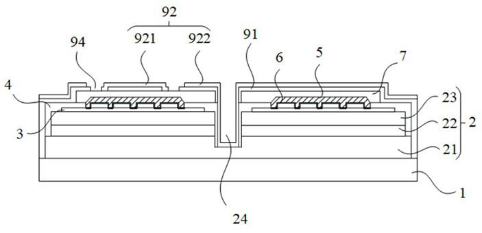
[0039] In order to facilitate the understanding of the present invention, the present invention will be described more fully below with reference to the associated drawings. Preferred embodiments of the invention are shown in the accompanying drawings. However, the present invention can be embodied in many different forms and is not limited to the embodiments described herein. On the contrary, these embodiments are provided to make the understanding of the disclosure of the present invention more thorough and comprehensive.

[0040] It should be noted that when an element is referred to as being “fixed” to another element, it can be directly on the other element or there can also be an intervening element. When an element is referred to as being "connected to" another element, it can be directly connected to the other element or intervening elements may also be present.

[0041] Unless otherwise defined, all technical and scientific terms used herein have the same meaning as...


PUM

PropertyMeasurementUnit
thicknessaaaaaaaaaa
thicknessaaaaaaaaaa
thicknessaaaaaaaaaa

Abstract

The invention relates to a light-emitting semiconductor and a preparation method thereof. The light-emitting semiconductor includes: a substrate, a light-emitting structure, a current spreading layer, a dielectric layer and a reflective layer sequentially stacked on the substrate along a direction close to the substrate, and is characterized in that, The dielectric layer is provided with a plurality of first through holes and grooves surrounding a circle, the plurality of first through holes and the grooves both penetrate the dielectric layer, the grooves extend circumferentially along the boundary of the closed figure, and the grooves surround the plurality of first through holes Set within the boundary of the closed figure, the periphery of the reflective layer falls into the groove. The present invention can use the groove to prevent the metal layer from gathering at the periphery of the photoresist, and avoid breakage after the subsequent film layer is covered; in addition, the groove can play the same conduction role as the first through hole, and does not affect the overall thickness of the insulating layer , so that the insulating layer can maintain an optimal thickness, which will neither affect the brightness extraction nor affect the electrode conduction.

Description

technical field [0001] The invention relates to the technical field of semiconductors, in particular to a light-emitting semiconductor and a preparation method thereof. Background technique [0002] Light Emitting Diode (LED for short) is a semiconductor light-emitting device with low energy consumption, long life, good stability, fast response, stable light-emitting wavelength and other photoelectric performance characteristics. It has been used in lighting, home appliances, display screens, There are a wide range of applications in areas such as indicator lights. Among them, the vertical and flip-chip LED structures have good current expansion performance and ohmic contact performance compared with the traditional front-mount LED structure, and are more used in high-power products. How to improve the light efficiency of LED chips is the direction of product research and development. The traditional reflection uses Ag reflection, and it is gradually proposed to use an omni...

Claims


Application Information

Patent Timeline
Patent Type & Authority Patents(China)
IPC IPC(8): H01L33/44H01L33/46H01L33/38H01L33/00
CPCH01L33/44H01L33/46H01L33/382H01L33/005
Inventor 徐晓丽李惠芸刘芳孙雷蒙杨丹
Owner HGC (WUHAN) TECH CO LTD
Why Eureka
Try Eureka