


Quick Research
Generate reliable direction feasibility study reports for your R&D in just a few steps.

Technical Q&A
Discover and master advanced knowledge NOW. Basics, ideas, possibilities, all at once.

Find Solutions
As an expert in R&D theories, this can generate solutions to your technical problems instantly.

Evaluate Feasibility
Analyze your overall solution with one click, know your potential R&D risks in advance.

Monitor Landscape
Get weekly tech updates, stay abreast of the latest tech innovations and key insights.
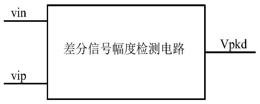
Input signal amplitude detection circuit with adjustable output signal range and method thereof
A technology of amplitude detection and output signal, which is applied in the field of input signal amplitude detection circuit, can solve the problems that the output signal range of the signal amplitude detection circuit cannot be adjusted, and cannot meet the signal amplitude detection indication of the ADC circuit, etc., so as to improve the detection range of the input signal and improve the The effect of linearity
- Summary
- Abstract
- Description
- Claims
- Application Information
AI Technical Summary
Problems solved by technology
Method used
Image

Examples
Embodiment 1
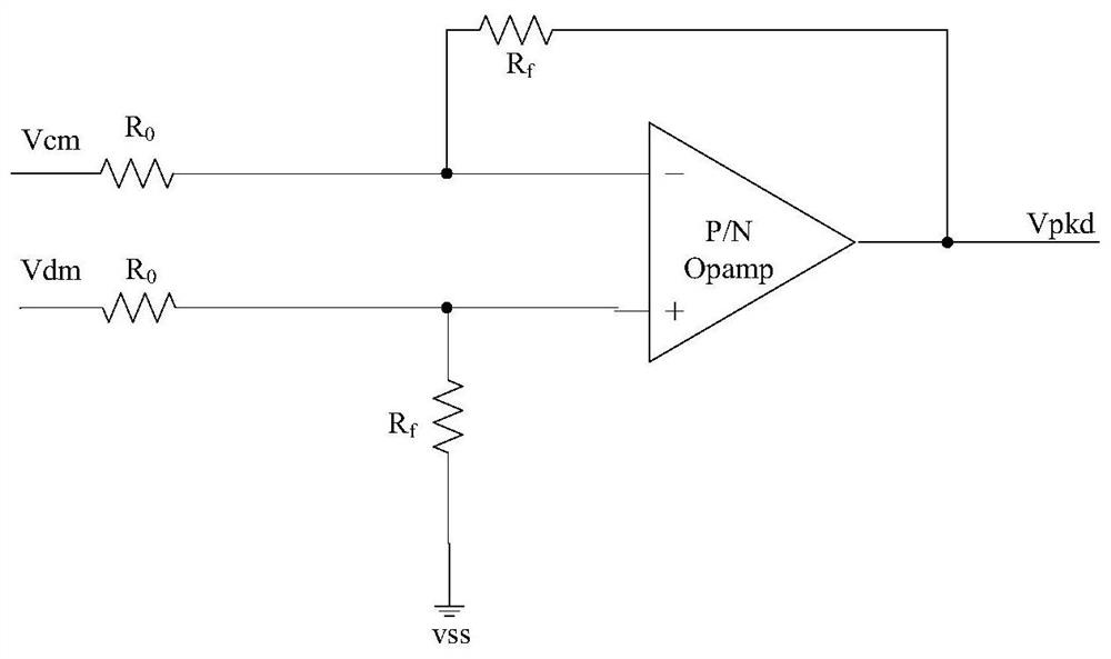
[0058] Embodiment 1 of the present invention provides an input signal amplitude detection circuit with adjustable output signal range, wherein the traditional error amplifier can refer to image 3 . And the embodiment of the present invention realizes as Figure 5 As shown, including the differential signal amplitude detection circuit and error amplifier, specifically:
[0059] The error amplifier circuit consists of resistors R 0 , R 01 ~R 0n and MOS switch sw 01 ~ sw 0n The first switched resistor array consisting of resistors R f , R f1 ~R fn and MOS switch sw f1 ~ sw fn A second switch resistor array formed, and an operational amplifier;
[0060] Wherein, the first switched resistor array is connected in series with the input negative pole or the input positive pole of the operational amplifier, or a set of the first switched resistor array is connected in series with the input positive pole and the input negative pole of the operational amplifier respectively; ...
Embodiment 2
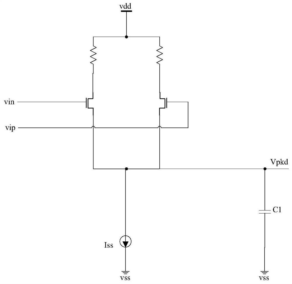
[0087] The embodiment of the present invention takes Figure 7 The differential signal amplitude detection circuit used in the present invention shown in figure 2 A source follower is added on the basis of , the function of this follower is to eliminate the V in formula ① th Influenced by the MOS tube V th Designed to be the same as the differential pair. The next step is to elaborate on its elimination of V th The principle and mechanism of the influence.
[0088] After the differential input signal passes through the signal amplitude detection circuit, two signals are output: the common mode output voltage V cm0 and differential mode output voltage V dm . in,
[0089]
[0090] V dm That is formula ①, from formula ①, V dm The result is simultaneously with the common mode component and differential mode components related, if the input signal amplitude is single-ended as V amp , ideally:
[0091] V in =V cm0 -V amp
[0092] V ip =V cm0 +V amp
[0093...
PUM
 Abstract
Description
Claims
Application Information
 - R&D Engineer
- R&D Manager
- IP Professional
- Industry Leading Data Capabilities
- Powerful AI technology
- Patent DNA Extraction
Browse by: Latest US Patents, China's latest patents, Technical Efficacy Thesaurus, Application Domain, Technology Topic, Popular Technical Reports.
© 2024 PatSnap. All rights reserved.Legal|Privacy policy|Modern Slavery Act Transparency Statement|Sitemap|About US| Contact US: help@patsnap.com