Chip packaging process

A chip packaging and process technology, used in semiconductor/solid-state device parts, semiconductor devices, electrical components, etc., can solve the problems of high chip cost, long baking time, and impact on chip performance.

Inactive Publication Date: 2021-12-17
NINGBO CRRC TIMES TRANSDUCER TECH CO LTD
View PDF4 Cites 0 Cited by
  • Summary
  • Abstract
  • Description
  • Claims
  • Application Information

AI Technical Summary

Problems solved by technology

[0006] (1) Due to the need to use the PCB board to complete the pin circuit conversion, the cost of the PCB board is increased;
[0007] (2) The existing structure adopts SMT patch technology, which has the risk of solder balls and virtual soldering;
[0008] (3) The cost of the chip is high, and poor molding and packaging will cause a large cost loss;
[0009] (4) After the chip, PCB board and PCB board pins are assembled, they need to be integrally molded and packaged. The high temperature and high pressure during molding will generate greater stress on the chip and PCB board, and affect the performance of the chip;
[0010] (5) The packaged chip needs to be baked, and the baking time is longer, which reduces the mass production efficiency

Method used


Image

  • Chip packaging process
  • Chip packaging process
  • Chip packaging process

Examples


Embodiment Construction

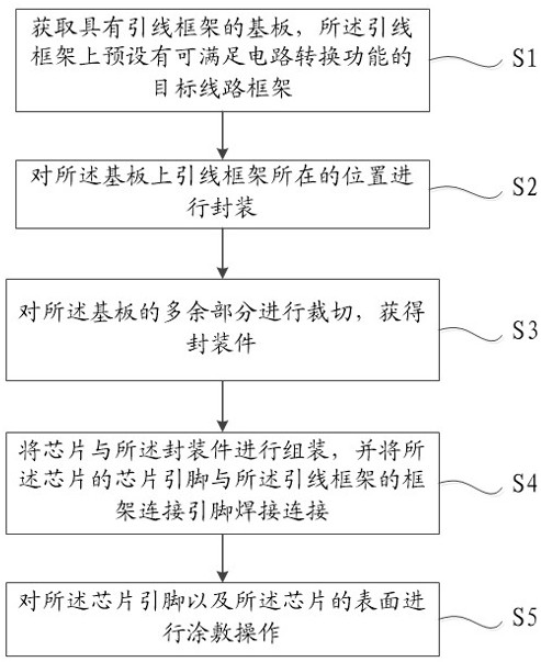
[0041] The core of the present invention is to provide a chip packaging process, which is used to reduce the cost, improve the production efficiency and ensure the performance of the chip.

[0042] In order to enable those skilled in the art to better understand the solution of the present invention, the present invention will be further described in detail below in conjunction with the accompanying drawings and specific embodiments.

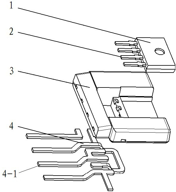
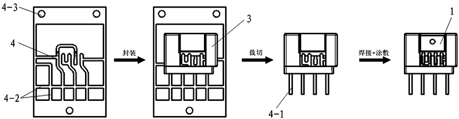
[0043] Please refer to Figure 1 to Figure 3 , figure 1 A flow chart of the chip packaging process provided by the present invention; figure 2 Schematic diagram of the structure of the chip, lead frame and package in the chip packaging process provided by the present invention; image 3 It is a process schematic diagram of the chip packaging process provided by the present invention.

[0044] In this embodiment, the chip packaging process includes the following steps:

[0045] Step S1: Obtain the substrate with the lead frame 4. The lead fr...


PUM


Abstract

The invention discloses a chip packaging process, which comprises the steps of obtaining a substrate with a lead frame, and presetting a target circuit frame capable of meeting a circuit conversion function on the lead frame; packaging the position of the lead frame on the substrate; cutting the redundant part of the substrate to obtain a packaging piece; assembling a chip and the packaging piece, and welding and connecting the chip pins of the chip with the frame connecting pins of the lead frame; and carrying out coating operation on the chip pins and the surface of the chip. According to the process provided by the invention, the target circuit frame is preset on the lead frame and can achieve a circuit conversion function; and a chip molding and packaging process is canceled, after the lead frame is directly packaged and molded, the chip and the packaging piece are welded and fixed, then coating treatment and single packaging are performed, and the chip pins and the frame connecting pins are connected by welding. The welding heat is low, the bonding strength is high, the connection strength is high after coating treatment, the insulation effect is good, and the reliability of the chip can be effectively improved.

Description

technical field [0001] The invention relates to the field of chip packaging, in particular to a chip packaging process. Background technique [0002] Current detection is an important function of the electric drive system of new energy vehicles, and its performance is directly related to the stability and reliability of electric vehicles. The current detection method based on the Hall current sensor has the advantages of low loss, stable performance, built-in isolation, and strong overload capability, and has gradually become the mainstream solution for current detection in new energy vehicles. Today, when new energy vehicle policy subsidies are decreasing year by year and market competition is becoming increasingly fierce, how to reduce the hard cost of products, ensure product reliability, and reduce production cycle are important items that need continuous improvement. [0003] Chip packaging refers to a process of plastic packages with different shapes formed by chips a...

Claims


Application Information

Patent Timeline
Patent Type & Authority Applications(China)
IPC IPC(8): H01L21/58H01L21/60H01L21/50H01L21/56H01L21/48H01L23/495
CPCH01L21/50H01L21/56H01L21/4842H01L23/495
Inventor 徐钉朱文琴王辰玥叶柳凯马华超胡玄张文江吴如兆
Owner NINGBO CRRC TIMES TRANSDUCER TECH CO LTD
Why Eureka
Try Eureka