Three-dimensional separated gate trench charge storage type IGBT and manufacturing method thereof

A technology of charge storage and charge storage layer, which is applied in the manufacture of circuits, electrical components, semiconductors/solid-state devices, etc., can solve problems such as increasing gate capacitance, deteriorating short-circuit safe working area, and slowing down the switching speed of devices. Forward conduction voltage drop, improve breakdown voltage and reliability, and reduce on-state loss

Active Publication Date: 2021-12-24
UNIV OF ELECTRONICS SCI & TECH OF CHINA
View PDF5 Cites 3 Cited by
  • Summary
  • Abstract
  • Description
  • Claims
  • Application Information

AI Technical Summary

Problems solved by technology

However, this method will increase the channel density, which will increase the saturation current on the one hand and deteriorate the short-circuit safe operating area (SCSOA) of the device; on the other hand, it will increase the gate capacitance, causing the device to switch The speed becomes slower and the switching loss increases

Method used


Image

  • Three-dimensional separated gate trench charge storage type IGBT and manufacturing method thereof
  • Three-dimensional separated gate trench charge storage type IGBT and manufacturing method thereof
  • Three-dimensional separated gate trench charge storage type IGBT and manufacturing method thereof

Examples


Embodiment Construction

[0078] The principles and features of the present invention are described below in conjunction with the accompanying drawings, and the examples given are only used to explain the present invention, and are not intended to limit the scope of the present invention.

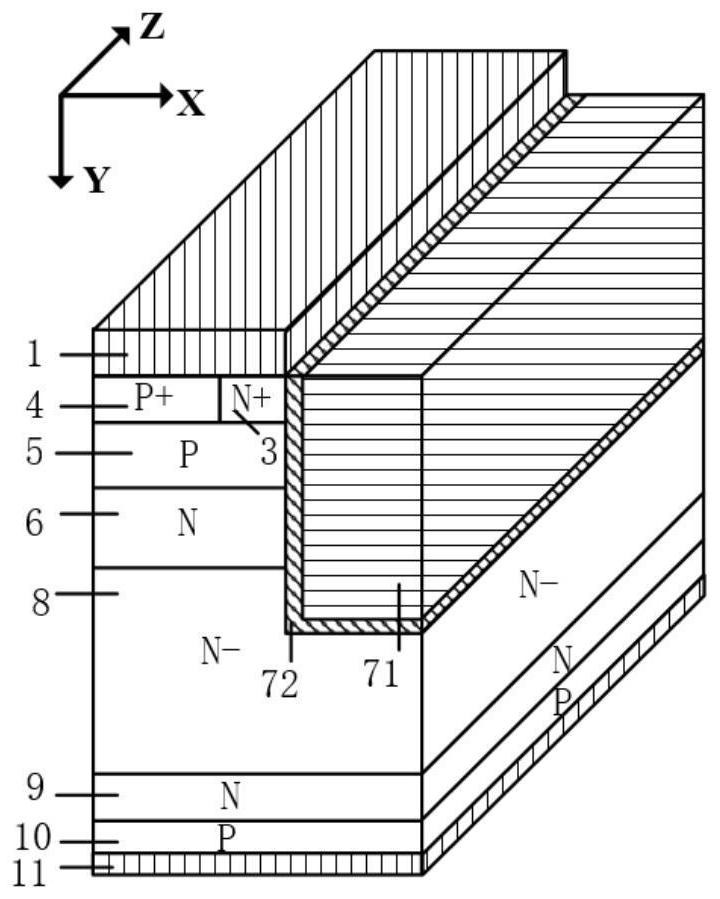
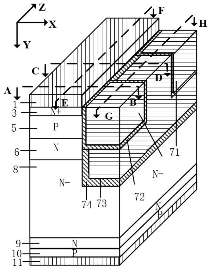
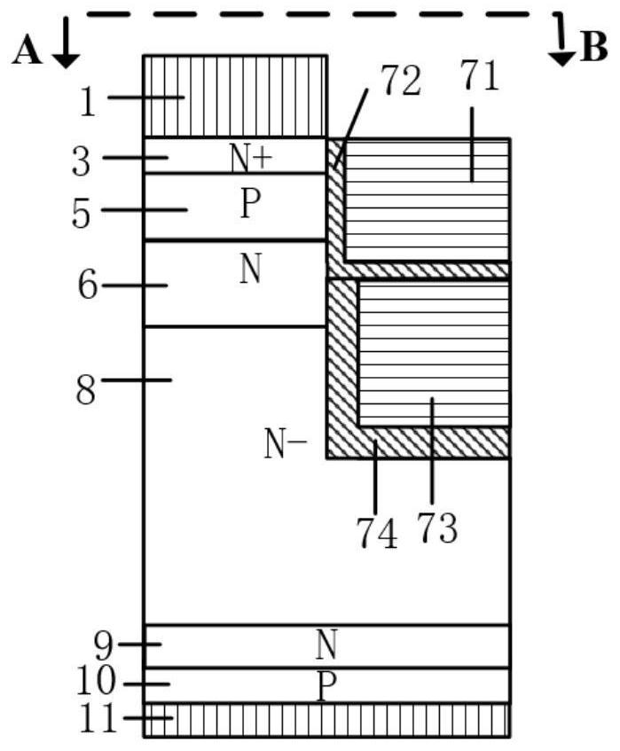
[0079] A three-dimensional separated gate trench charge storage type IGBT provided by Embodiment 1 of the present invention, its half-cell structure and the cross-sections along AB line, CD line, EF line and GH line are as follows: Figure 2-6 as shown,

[0080] Define the three-dimensional direction of the device with a three-dimensional rectangular coordinate system: define the horizontal direction of the device as the X-axis direction, the vertical direction of the device as the Y-axis direction, and the longitudinal direction of the device, that is, the third dimension direction, as the Z-axis direction. The cell structure includes: along the Y-axis axis direction, the back collector metal 11, P-type collector r...


PUM

PropertyMeasurementUnit
thicknessaaaaaaaaaa
thicknessaaaaaaaaaa
thicknessaaaaaaaaaa

Abstract

The invention relates to a three-dimensional separated gate trench charge storage type IGBT and a manufacturing method thereof, and belongs to the technical field of power semiconductor devices. According to the present invention, a P-type buried layer and a separated gate electrode equipotential with the emitter metal are introduced on the basis of a traditional CSTBT, the influence of the doping concentration of an N-type charge storage layer on the breakdown characteristic of a device is effectively eliminated through charge compensation, and meanwhile, the conduction voltage drop can be reduced by improving the doping concentration of the N-type charge storage layer. According to the present invention, the gate electrodes and the separated gate electrodes are placed in a same groove, and the gate electrodes are arranged at intervals along the Z-axis direction, so that on one hand, the channel density can be reduced, on the other hand, a parasitic PMOS structure can be formed in a cell, the saturation current density can be reduced, and a short-circuit safe working area can be improved; and meanwhile, the gate capacitance and gate charge are reduced, the switching loss of the device is reduced, the compromise relationship between the forward conduction voltage drop Vceon and the turn-off loss Eoff is further improved; and in addition, the improvement of the current uniformity and the improvement of the reliability of the device are also facilitated.

Description

technical field [0001] The invention belongs to the technical field of power semiconductor devices, and in particular relates to a three-dimensional separated gate trench charge storage type IGBT and a manufacturing method thereof. Background technique [0002] Insulated Gate Bipolar Transistor (IGBT) is one of the fastest growing electronic power devices today. Compared with traditional transistors and MOSFETs, it has the advantages of both transistors and MOSFETs. It not only has the advantages of high input impedance, low control power, simple driving circuit, fast switching speed, and low switching loss of MOSFET; it also has the advantages of bipolar Power transistors have the advantages of high current density, low saturation voltage, strong current handling capability, and good stability, so they are widely used in high voltage, high current and other fields. [0003] Since the IGBT was invented in the late 1970s and early 1980s, people have been committed to improvi...

Claims


Application Information

Patent Timeline
Patent Type & Authority Applications(China)
IPC IPC(8): H01L29/06H01L29/423H01L29/739H01L21/28H01L21/331
CPCH01L29/7398H01L29/7397H01L29/66348H01L29/0684H01L29/0623H01L29/401H01L29/42312H01L29/0696
Inventor 张金平朱镕镕涂元元李泽宏张波
Owner UNIV OF ELECTRONICS SCI & TECH OF CHINA
Why Eureka
Try Eureka