Semiconductor device as well as application and manufacturing method thereof

A semiconductor and device technology, applied in the field of semiconductor devices and its application and manufacturing, can solve the problems of low hole mobility, difficulty in forming integrated high-performance logic circuits and reverse amplifiers, and difficulty in achieving high P-type doping, etc. Achieve the effect of improving quality, reducing source-drain spacing, and improving hole mobility

Pending Publication Date: 2022-01-04
SHENZHEN JING XIANG TECH CO LTD
View PDF0 Cites 1 Cited by
  • Summary
  • Abstract
  • Description
  • Claims
  • Application Information

AI Technical Summary

Problems solved by technology

Due to the low hole mobility in Gallium Nitride, it is difficult to achieve high P-type doping in this material, and the lack of monolithic complementary P-type Field Effect Transistor (Field Effect Transistor, FET), it is difficult to form an integrated high-performance logic circuit and inverting amplifier stage

Method used


Image

  • Semiconductor device as well as application and manufacturing method thereof
  • Semiconductor device as well as application and manufacturing method thereof
  • Semiconductor device as well as application and manufacturing method thereof

Examples


Embodiment Construction

[0053] The following will clearly and completely describe the technical solutions in the embodiments of the present invention with reference to the accompanying drawings in the embodiments of the present invention. Obviously, the described embodiments are only some, not all, embodiments of the present invention. Based on the embodiments of the present invention, all other embodiments obtained by persons of ordinary skill in the art without creative efforts fall within the protection scope of the present invention.

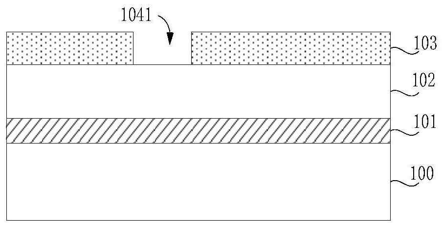
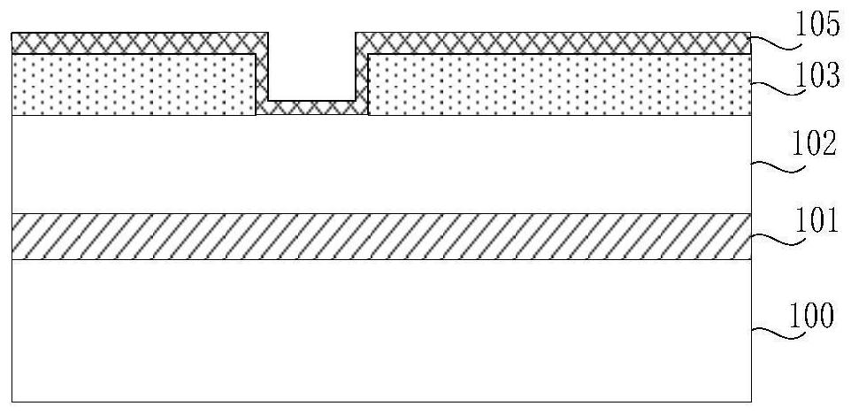
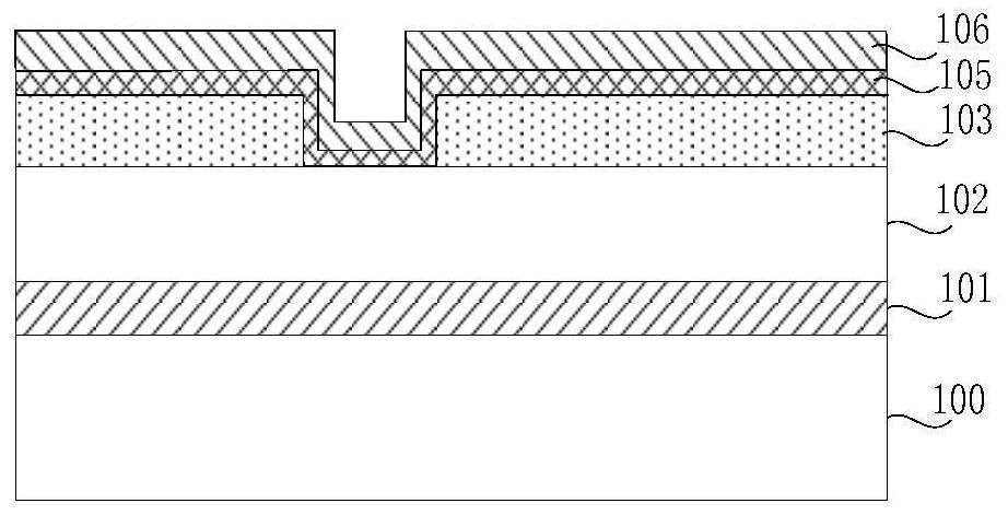
[0054] see Figure 1 to Figure 36 As shown, the semiconductor device or monolithically integrated semiconductor device provided by the present invention includes a substrate 100, an epitaxial structure disposed on the substrate 100, and a source 107, a drain 108 and a gate 109 disposed on the epitaxial structure . Wherein, the epitaxial structure includes a heterostructure formed by gallium nitride and aluminum gallium nitride (GaN / AlGaN). And in this application...


PUM

PropertyMeasurementUnit
thicknessaaaaaaaaaa
thicknessaaaaaaaaaa
thicknessaaaaaaaaaa

Abstract

The invention discloses a semiconductor device as well as application and a manufacturing method thereof. The semiconductor device comprises a substrate, a channel layer arranged on the substrate, a potential barrier layer arranged on the channel layer, a first gallium nitride layer which is arranged on the barrier layer and covers the barrier layer, a second gallium nitride layer which is arranged on the first gallium nitride layer, a third gallium nitride layer which is arranged on the second gallium nitride layer, a first drain electrode which is arranged on the third gallium nitride layer, a first source electrode which is arranged on the third gallium nitride layer, and a first grid electrode which is arranged on the barrier layer; a concave part is formed between the first source electrode and the first drain electrode; the first grid electrode covers the concave part; the first source electrode and the first drain electrode are close to the top of the concave part; the second gallium nitride layer and the third gallium nitride layer are located between the source electrode and the barrier layer and between the drain electrode and the barrier layer. According to the semiconductor device provided by the invention, the quality of the integrated semiconductor device can be improved.

Description

technical field [0001] The invention belongs to the technical field of semiconductors, in particular to a semiconductor device and its application and manufacturing method. Background technique [0002] As a wide bandgap semiconductor, gallium nitride has the characteristics of high breakdown electric field, high electron saturation velocity and mobility, so gallium nitride-based power devices can be used in the preparation of a new generation of high-power converters. The current gallium nitride-based power The device is a lateral heterojunction AlGaN / GaN high electron mobility transistor device. Due to the low hole mobility in Gallium Nitride, it is difficult to achieve high P-type doping in this material, and the lack of monolithic complementary P-type Field Effect Transistor (Field Effect Transistor, FET), it is difficult to form an integrated high-performance logic circuits and inverting amplifier stages. Contents of the invention [0003] The object of the present ...

Claims


Application Information

Patent Timeline
Patent Type & Authority Applications(China)
IPC IPC(8): H01L29/778H01L21/335H01L29/06
CPCH01L29/7783H01L29/7786H01L29/66462H01L29/0603H01L29/0684
Inventor 林信南石黎梦
Owner SHENZHEN JING XIANG TECH CO LTD
Why Eureka
Try Eureka