
Energy-saving and environment-friendly efficient waste LED chip recovery processing device

An LED chip, energy-saving and environmentally friendly technology, applied in the field of high-efficiency recycling and processing devices, can solve the problems of unfavorable devices such as long-time processing, time-consuming and material resources, and slow recycling and processing efficiency, so as to achieve high maintenance and update performance, enhanced processing effect, and easy recycling. Effect of treatment

Active Publication Date: 2022-01-11
江苏荣麒循环科技有限公司
View PDF24 Cites 1 Cited by
  • Summary
  • Abstract
  • Description
  • Claims
  • Application Information

AI Technical Summary

Problems solved by technology

[0003] In the prior art, the recovery and treatment devices used for waste LED chips need a lot of time and material resources, and the separated structural liquid is likely to pollute the surrounding environment, and most of the ordinary recovery treatment devices recycle the overall structure of the chips, and the separation effect Poor, so that the chips need to be manually assisted screening, the recycling efficiency is slow, and when the efficient recycling operation is carried out, the structure is often blocked due to the accumulation of electronic components, resulting in the need for maintenance of the device, which is not conducive to the long-term processing of the device

Method used


Image

  • Energy-saving and environment-friendly efficient waste LED chip recovery processing device
  • Energy-saving and environment-friendly efficient waste LED chip recovery processing device
  • Energy-saving and environment-friendly efficient waste LED chip recovery processing device

Examples


Embodiment Construction

[0030] The following will clearly and completely describe the technical solutions in the embodiments of the present invention with reference to the accompanying drawings in the embodiments of the present invention. Obviously, the described embodiments are only some, not all, embodiments of the present invention. Based on the embodiments of the present invention, all other embodiments obtained by persons of ordinary skill in the art without making creative efforts belong to the protection scope of the present invention.

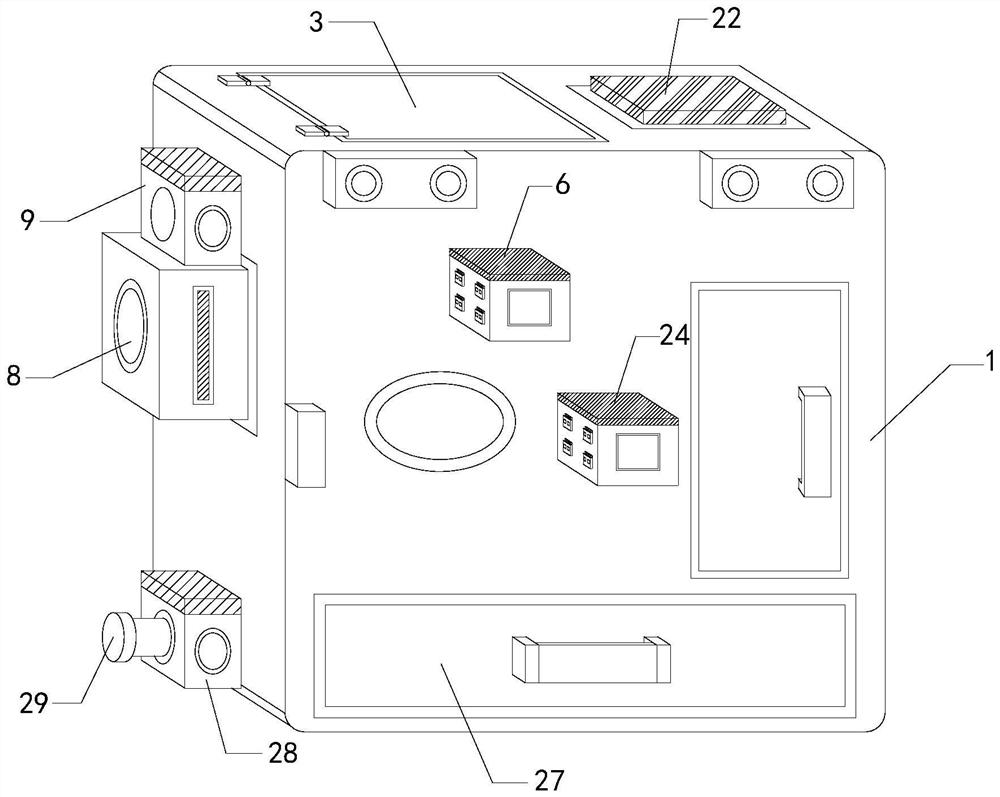
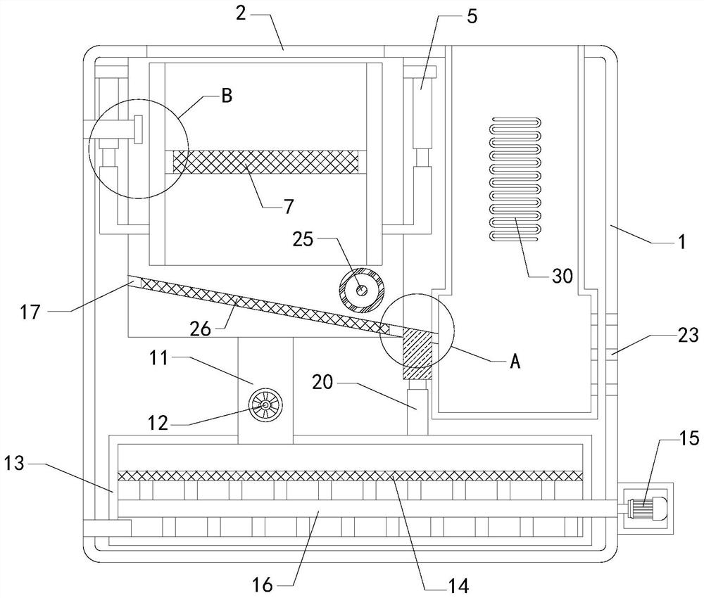
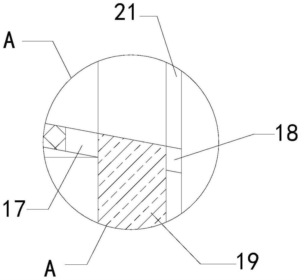
[0031] see Figure 1-7 , the present invention discloses a high-efficiency recycling and processing device based on energy-saving and environmental-friendly waste LED chips, which includes a box body 1, a through groove 2 is opened on the top of the box body 1, and a cover is movably arranged on the top of the inner wall of the through groove 2 Plate 3, the inner wall of the through groove 2 is provided with a shelf 4, and the bottom of both sides of the top o...


PUM


Abstract

The invention discloses an energy-saving and environment-friendly efficient waste LED chip recovery processing device, and relates to the technical field of chip recovery. The device comprise as box body, a through groove is formed in the top of the box body, a cover plate is movably arranged at the top of the inner wall of the through groove, a placing frame is movably arranged on the inner wall of the through groove, air cylinders are fixedly arranged at the bottoms of the two sides of the top of the placing frame, a first motor is movably arranged on the front surface of the placing frame, a first screen is fixedly arranged on an output shaft of the first motor, a storage box is fixedly arranged on one side of the box body, and a first water pump is fixedly arranged at the top of the storage box. A stirrer and a second screen are movably arranged, so that a solution in a collecting box can be separated from electronic elements, a second water pump can collect the solution in the collecting box, the recovery effect is enhanced, a liquid outlet can be used for discharging through the second water pump, the recovery processing capacity of the device is comprehensively improved, and energy saving and environmental protection are achieved.

Description

technical field [0001] The invention relates to the technical field of chip recycling, in particular to an efficient recycling and processing device based on energy-saving and environment-friendly waste LED chips. Background technique [0002] A solid-state semiconductor device. The heart of the LED is a semiconductor wafer. One end of the wafer is attached to a bracket, one end is the negative pole, and the other end is connected to the positive pole of the power supply, so that the entire wafer is encapsulated by epoxy resin. Also known as LED light-emitting chip, it is the core component of LED lights, which refers to the P-N junction. Its main function is to convert electrical energy into light energy, and the main material of the chip is monocrystalline silicon. Semiconductor wafer is made up of two parts, and a part is P-type semiconductor, and hole occupies an leading position in it, and the other end is N-type semiconductor, and here mainly is electron. But time th...

Claims


Application Information

Patent Timeline
IPC IPC(8): B09B3/30B09B3/70B09B3/40B01D36/00F26B21/00B09B101/15
CPCB09B3/00B01D36/00F26B21/004F26B21/001F26B2200/04Y02W30/82
Inventor 王朝君
Owner 江苏荣麒循环科技有限公司
Learn More