Ultraviolet LED and detector homogeneous integrated chip and preparation method thereof

A technology of integrated chips and LED devices, applied in the field of semiconductor technology and communication, can solve the problems affecting the transmission rate, bandwidth and power consumption of integrated chips, low optical coupling efficiency, low response efficiency, etc., to improve signal conversion efficiency and transmission speed. , the preparation process is simple and the sensitivity is improved

Pending Publication Date: 2022-01-18
CHANGCHUN INST OF OPTICS FINE MECHANICS & PHYSICS CHINESE ACAD OF SCI
View PDF0 Cites 0 Cited by
  • Summary
  • Abstract
  • Description
  • Claims
  • Application Information

AI Technical Summary

Problems solved by technology

[0003] However, previous research on homogenous integrated chips of LEDs and detectors found that due to the uncertainty of the light output direction of the light source, only a very small part of the light propagating through the air can be detected by PDs. The traditional solution is to use optical waveguides to limit the optical path. Auxiliary light transmission, but because the waveguide device generally only has a single directionality, and the optical coupling efficiency between the light source and the detector is low, the loss of the optical signal is still serious, resulting in weak collection ability on the detector side and low response efficiency. Ultimately affect the transmission rate, bandwidth and power consumption of the integrated chip

Method used


Image

  • Ultraviolet LED and detector homogeneous integrated chip and preparation method thereof
  • Ultraviolet LED and detector homogeneous integrated chip and preparation method thereof
  • Ultraviolet LED and detector homogeneous integrated chip and preparation method thereof

Examples


Embodiment Construction

[0045] Embodiments of the present application are described in detail below, examples of which are shown in the drawings, wherein the same or similar reference numerals denote the same or similar elements or elements having the same or similar functions throughout. The embodiments described below by referring to the figures are exemplary only for explaining the present invention and should not be construed as limiting the present application.

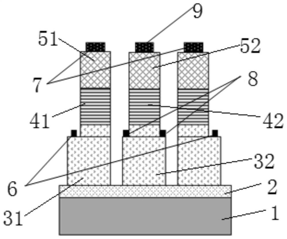
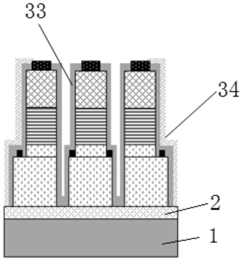
[0046] like Figure 1~2 As shown, the embodiment of the present application provides a homogeneous integrated chip of ultraviolet LED and detector, including:

[0047] substrate1;

[0048] buffer layer 2, which is located on one side of the substrate 1;

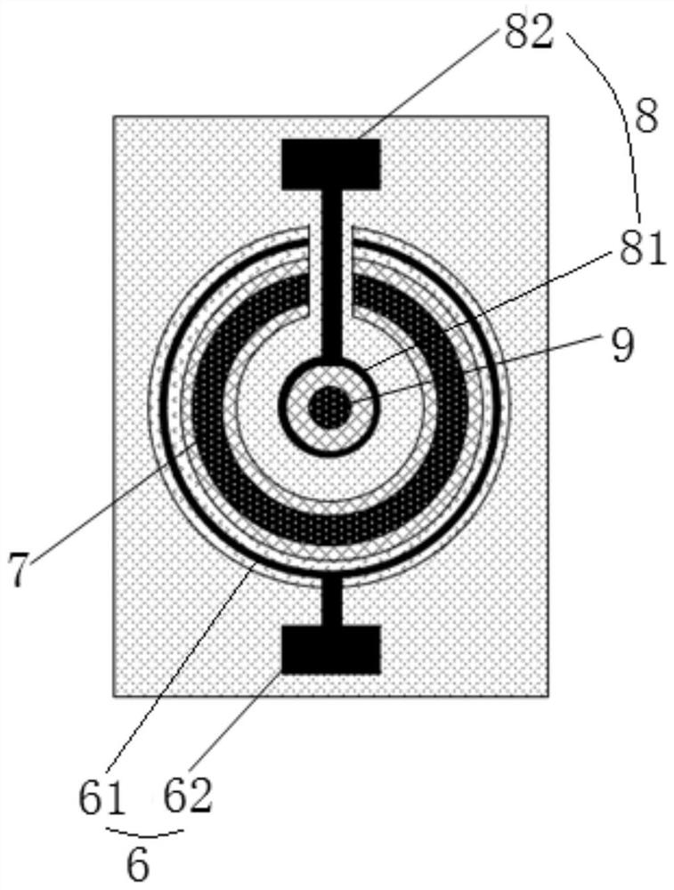
[0049] The LED device is located on the side of the buffer layer 2 away from the substrate 1, and the LED device is in the shape of a ring or an arc;

[0050] The detector is located on the side of the buffer layer 2 away from the substrate 1 and inside the LED device.

[0051]It s...


PUM

PropertyMeasurementUnit
thicknessaaaaaaaaaa
thicknessaaaaaaaaaa
thicknessaaaaaaaaaa

Abstract

The invention provides an ultraviolet LED and detector homogeneous integrated chip and a preparation method thereof, and the homogeneous integrated chip comprises a substrate; a buffer layer; an LED device which is in a circular ring shape or a circular arc shape; and a detector positioned on the inner side of the LED device. According to the integrated chip, the circular-ring-shaped or circular-arc-shaped LED device and the detector located on the inner side of the LED device are adopted, the utilization rate of light emitted by the LED is increased in the direction, the interaction area of the LED and the side wall of the detector is increased under the condition that the area of an active area is fixed, and collection of the detector is facilitated. According to the integrated chip, a metal reflecting layer is arranged on the peripheral surface of the LED device, so that the light extraction efficiency and the electro-optical conversion efficiency of the LED device in the homogeneous integrated chip are greatly improved, the incident luminous flux received by a detector is increased, the sensitivity is improved, and the light dissipation of the integrated chip is effectively reduced. Therefore, the purpose of improving the signal conversion efficiency and the transmission speed of the homogeneous integrated chip of the ultraviolet LED and the detector is achieved.

Description

technical field [0001] The invention relates to the field of semiconductor technology and communication, in particular to a homogeneous integrated chip of an ultraviolet LED and a detector and a preparation method thereof. Background technique [0002] Because ultraviolet light has the advantages of short wavelength, high frequency, fast transmission speed, and no interference from visible light, it is easy to conceal and has good confidentiality. It has great application value in the fields of guidance, atmospheric environment monitoring, deep space exploration and ultraviolet navigation. AlGaN is a direct bandgap semiconductor, its bandgap width is continuously adjustable between 3.4-6.2eV with the change of Al composition, the corresponding wavelength is 365nm-200nm, covering most of the ultraviolet band, and has stable physical and chemical properties. It can work under the conditions of high frequency, high voltage and high power, and is a high-quality material for pre...

Claims


Application Information

Patent Timeline
Patent Type & Authority Applications(China)
IPC IPC(8): H01L27/144H01L27/15H01L31/0352H01L33/06H01L33/38H01L33/46
CPCH01L27/1443H01L27/153H01L33/06H01L33/46H01L33/38H01L31/035263
Inventor 孙晓娟陈雨轩黎大兵蒋科贲建伟石芝铭
Owner CHANGCHUN INST OF OPTICS FINE MECHANICS & PHYSICS CHINESE ACAD OF SCI
Why Eureka
Try Eureka