
Active semiconductor nuclear radiation detector for converting nuclear radiation into luminescence

A semiconductor and N-type semiconductor technology, applied in the field of nuclear radiation detection, can solve the problems of slow decay time, low luminous efficiency, difficult to control, etc., and achieve the effect of improving the overall efficiency, high luminous efficiency, and high-efficiency conversion

Pending Publication Date: 2022-01-18
NORTHWEST INST OF NUCLEAR TECH
View PDF0 Cites 0 Cited by
  • Summary
  • Abstract
  • Description
  • Claims
  • Application Information

AI Technical Summary

Problems solved by technology

After a century of research, the types of scintillators have been enriched and developed, and the performance of scintillators has been greatly improved, but scintillators with high luminous efficiency and fast luminous time are still an elusive dream
In the existing scintillators, it is often difficult to balance the luminous efficiency and speed. For example, the luminous time of wide bandgap semiconductor materials such as ZnO and CuI can reach sub-nanoseconds, but the luminous efficiency is particularly low; while SrI 2 (Eu) The light yield exceeds 85000ph / MeV, but the decay time is as slow as microseconds
[0003] The luminescence of scintillators mainly depends on the properties of the material itself, which is difficult to control. Artificial intervention usually increases the luminescence speed at the expense of the light yield. For example, heating the YAG crystal will shorten the decay time significantly, but the luminous efficiency will also decrease.
There are also studies using quantum confinement effects, plasmons and other designs to accelerate the luminescence transition process, but the efficiency is still very low

Method used


Image

  • Active semiconductor nuclear radiation detector for converting nuclear radiation into luminescence
  • Active semiconductor nuclear radiation detector for converting nuclear radiation into luminescence
  • Active semiconductor nuclear radiation detector for converting nuclear radiation into luminescence

Examples


Embodiment Construction

[0029] Now in conjunction with embodiment, accompanying drawing, the present invention will be further described:

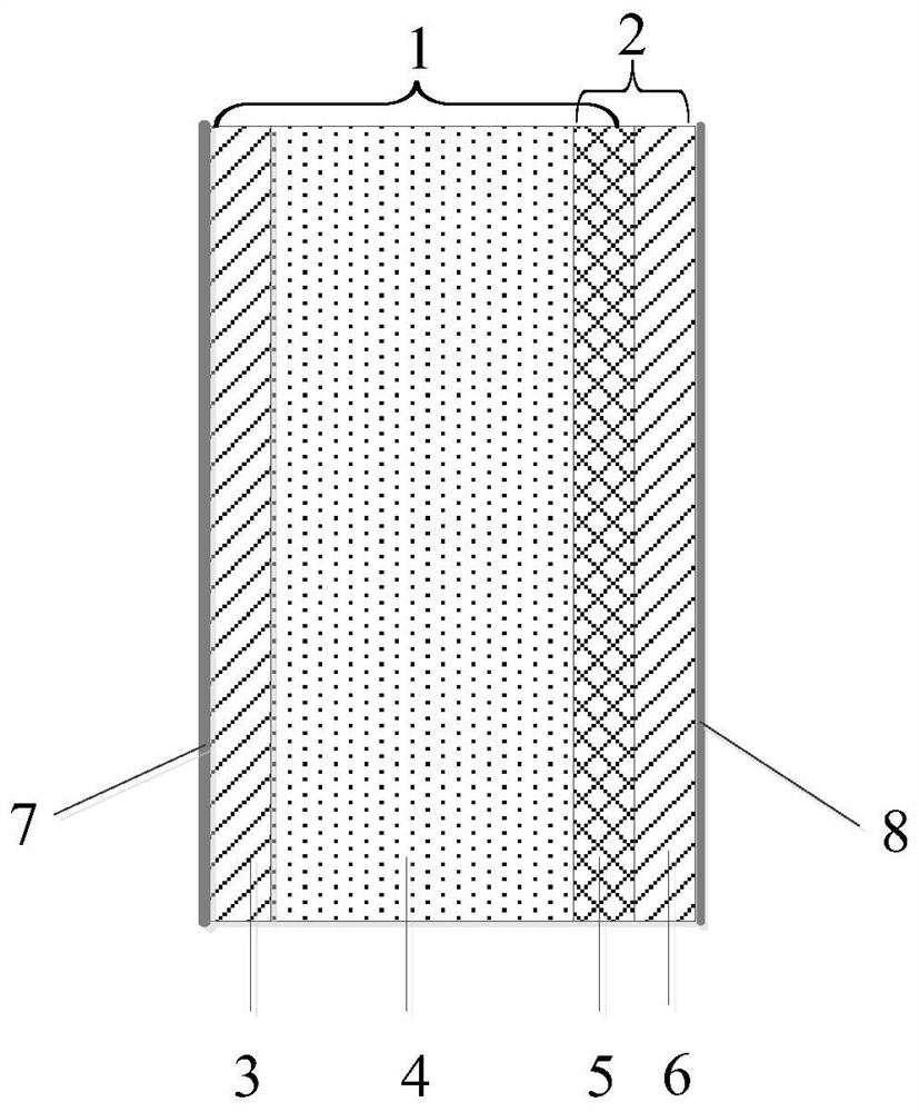
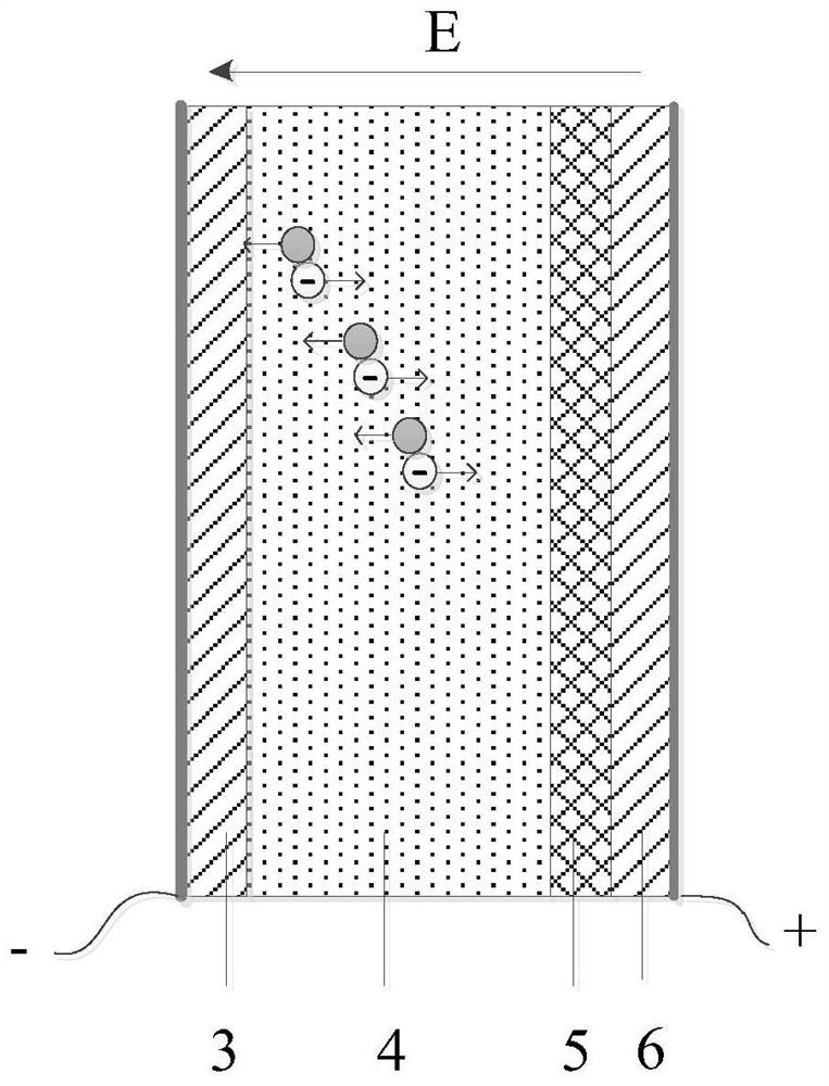
[0030] The electro-optic coupling nuclear radiation detection device of the embodiment of the present invention has a main body structure of a flat plate, which is composed of a PIN structure 1 and an LED light-emitting diode 2 connected in series, both of which share an N layer or a P layer. It is characterized in that, if the N layer is shared, the PIN structure 1 is composed of P-type semiconductor material 3, intrinsic semiconductor material 4 and N-type semiconductor material 5; the LED light-emitting diode 2 is composed of N-type semiconductor material 5 and P-type semiconductor material Material 6 composition. Multiple layers of different types of semiconductor materials are stacked to form a PINP structure, and electrodes 7 and 8 are respectively fabricated on the surface of the device.

[0031] The PIN structure 1 and the LED light-emitting diode 2 are ...


PUM

PropertyMeasurementUnit
Thicknessaaaaaaaaaa
Thicknessaaaaaaaaaa

Abstract

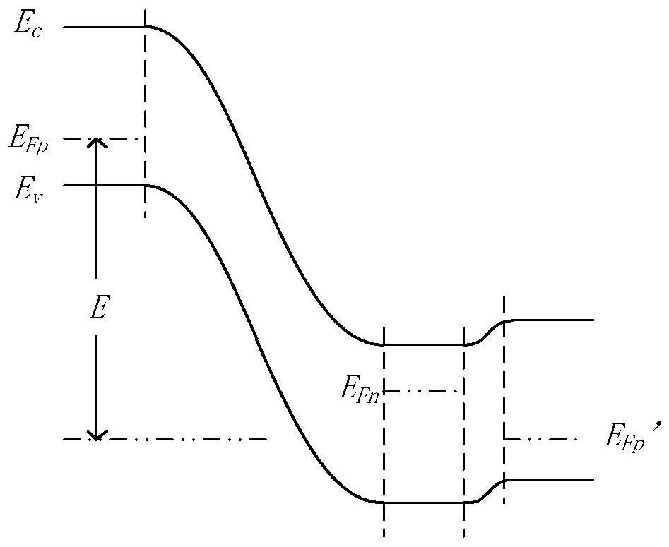
The invention relates to an active semiconductor nuclear radiation detection device for converting nuclear radiation into light emission. The active semiconductor nuclear radiation detection device comprises a PIN structure and an LED light emitting diode; the two PIN structure and the LED light emitting diode are serially connected, and the series connection areas share one N layer or P layer; and electrodes are respectively manufactured on the surface of the device. A traditional PIN semiconductor detector technology is combined with an LED light-emitting structure, energy deposition under the action of rays is completed through a reverse-biased PIN junction, carriers are generated, and the carriers enter an LED under the action of an electric field and are converted into light to be output in a composite light-emitting area, so that nuclear-electricity-light conversion detection is achieved. Therefore, a novel semiconductor active device for nuclear radiation detection is formed. Compared with an uncontrolled light-emitting process of a scintillator, the novel device is an active device, effective control over the carrier transport and carrier composite light-emitting process can be achieved through structural design and adjustment of an external electric field, and then the control over the nuclear-electricity-light conversion detection process is achieved.

Description

technical field [0001] The invention belongs to nuclear radiation detection technology, and relates to an active semiconductor nuclear radiation detection device that converts nuclear radiation into luminescence, which can replace the function of a traditional scintillator. Background technique [0002] Scintillator is a very important basic material for nuclear radiation detection. Its function is to convert high-energy particles and rays into light. The detection of high-energy particles and rays can be realized by measuring the luminescence of scintillators. It is used in high-energy physics and nuclear physics experiments, It is widely used in nuclear medical imaging, environmental monitoring gamma energy spectroscopy and other fields, and it is also an indispensable key material for neutrons in pulsed radiation fields, gamma diagnosis and construction of pulsed radiation imaging systems. Luminescence efficiency and luminescence time are two important parameters of scint...

Claims


Application Information

Patent Timeline
IPC IPC(8): H01L31/12H01L31/117H01L31/153
CPCH01L31/125H01L31/153H01L31/117
Inventor 陈亮周磊簜欧阳晓平卢星王晶
Owner NORTHWEST INST OF NUCLEAR TECH
Learn More