
Power semiconductor device and manufacturing method thereof

A technology of power semiconductors and manufacturing methods, which is applied to semiconductor devices, electrical solid devices, electrical components, etc., can solve the problems of low utilization rate of silicon carbide chips, large loss of freewheeling diodes, and low channel mobility, etc., to avoid dual Extremely degraded effect, improved surge capability, enhanced robustness effect

Pending Publication Date: 2022-01-21
湖南国芯半导体科技有限公司
View PDF0 Cites 0 Cited by
  • Summary
  • Abstract
  • Description
  • Claims
  • Application Information

AI Technical Summary

Problems solved by technology

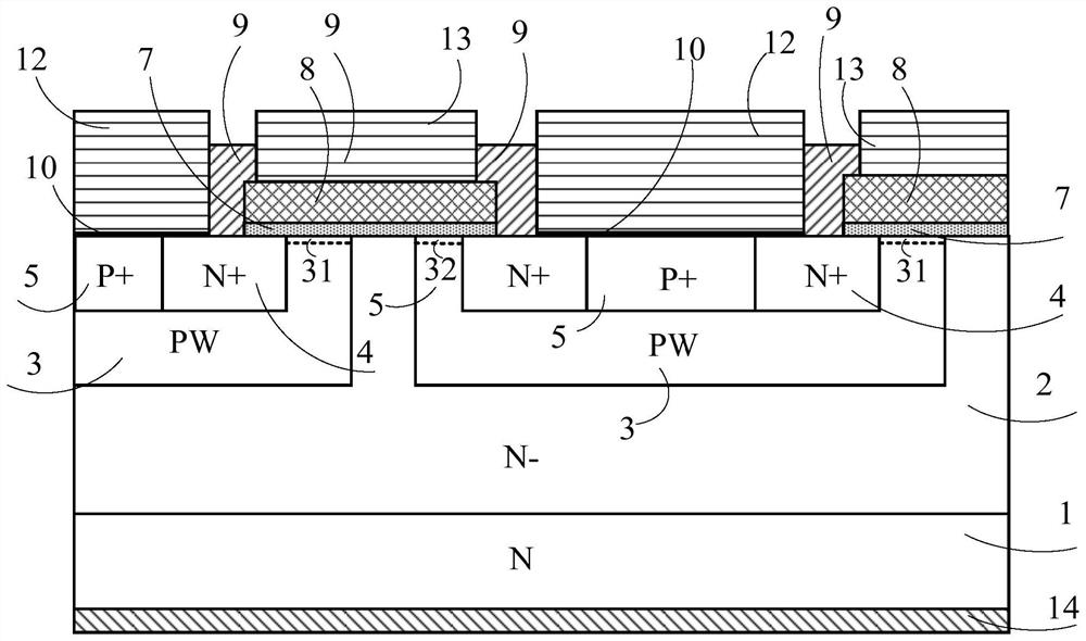
Low channel mobility is the key factor for the large on-resistance of silicon carbide planar gate MOSFETs. At the same time, silicon carbide can only be implanted with ions. The N+ source region and P-type well PW of planar gate MOSFETs use two-layer photolithographic registration. , due to easy misalignment, the overlay deviation will cause the channel length of the two half-cells (eg figure 1 Shown in 31 and 32) is asymmetrical, causing the conduction current of the device to select the shorter channel to flow to the drain, and half of the cells of the longer channel are not used
[0005] In summary, the current power MOSFET devices have defects such as large gate-to-drain charge, low utilization rate of silicon carbide chips, and large loss of freewheeling diodes.

Method used


Image

  • Power semiconductor device and manufacturing method thereof
  • Power semiconductor device and manufacturing method thereof
  • Power semiconductor device and manufacturing method thereof

Examples


Embodiment 1

[0059] Step 1: Using an epitaxial process, an N-type epitaxial layer 2 is formed on a silicon carbide N-type substrate 1, wherein the resistivity of the N-type substrate 1 is 0.01-0.03Ω.cm, and the thickness is 200-400 μm. The doping concentration of layer 2 is 5e14~5e16cm -3 ;

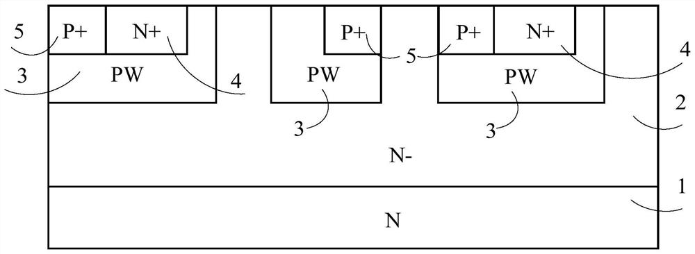
[0060] Step 2: Form a P base region 3 above the N-type epitaxial layer 2 by using photolithography and ion implantation technology, the junction depth of the P base region 3 is 0.6-1.5um, and the peak doping concentration is 1e18-5e19cm -3 , forming an N+ source region 4 in the P base region 3, with a junction depth of 0.2-0.5um and a peak doping concentration of 5e18-5e20cm -3 , forming a P+ source region 5 in the P base region 3, the junction depth is 0.2-0.5um, and the doping concentration is 5e18-5e20cm -3 , and activate the impurities in the above-mentioned implanted regions by high-temperature annealing, such as image 3 shown;

[0061] Step 3: Deposit a layer of insulating dielectric materi...

Embodiment 2

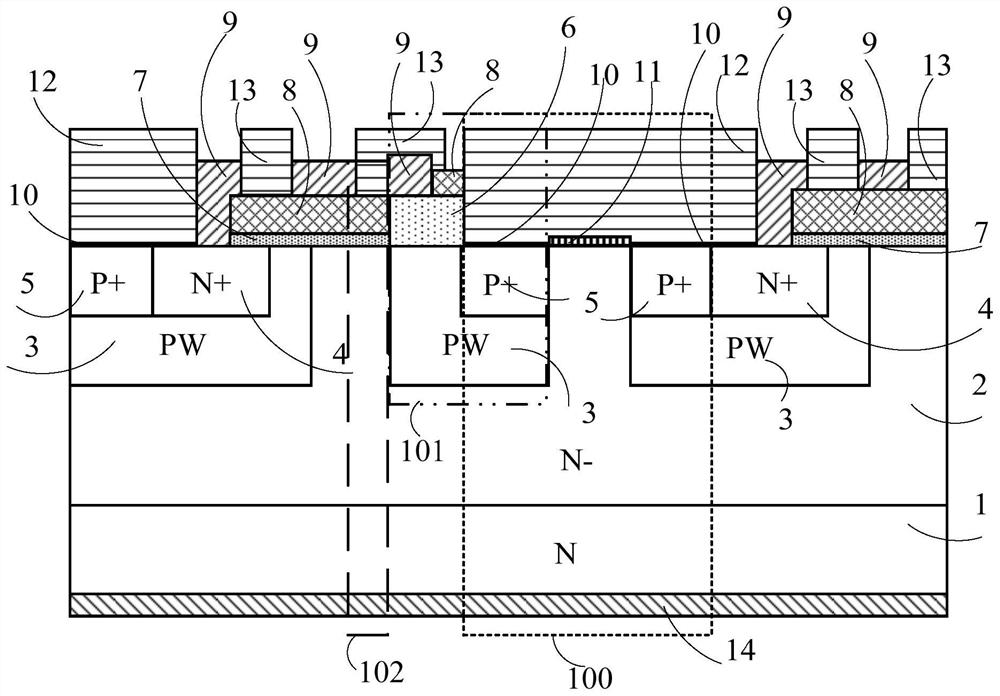
[0071] Same as Embodiment 1, all utilize MOSFET half-cells to integrate MPS ( Figure 8 Middle dotted line frame 200); The difference from Embodiment 1 is that by removing a piece of polysilicon 8 ( Figure 8 There is no polysilicon 8 in the dotted line frame 201) and the size of the working gate is reduced, the gate charge is reduced, and the PMOS capacitor is not formed in the MPS part, as Figure 8 shown.


PUM

PropertyMeasurementUnit
Doping concentrationaaaaaaaaaa
Knot deepaaaaaaaaaa
Thicknessaaaaaaaaaa

Abstract

The invention discloses a power semiconductor device and a manufacturing method thereof, the power semiconductor device comprises a silicon carbide N-type substrate, an N-type epitaxial layer is arranged on the silicon carbide N-type substrate, a P base region is arranged on the N-type epitaxial layer, an N + source region and a P + source region are formed in the P base region to form an intermediate device, and a P + source region is formed in the P base region. An insulating medium material layer and a gate medium material layer are deposited on the surface of the intermediate device, polycrystalline silicon is deposited on the insulating medium material layer and the gate medium material layer, ohmic contact layers are formed on the surfaces of the N + source region and the P + source region, and a Schottky contact layer is formed on the surface of the N-type epitaxial layer between the P + source region and the P + source region. Source electrodes are arranged on the ohmic contact layer and the Schottky contact layer, a grid electrode is arranged on the polycrystalline silicon, and a drain electrode is arranged on the back face of the silicon carbide N-type substrate. The anti-parallel diode has the advantages of reducing gate leakage charge, improving the chip utilization rate, reducing the loss of the anti-parallel diode, improving the surge capacity of the anti-parallel diode and the like.

Description

technical field [0001] The invention mainly relates to the technical field of semiconductors, in particular to a power semiconductor device and a manufacturing method thereof. Background technique [0002] Power MOSFET devices In switching applications, the gate charge must be overcome to regulate the transistor to a specific voltage, and the switching speed of the transistor decreases significantly at larger gate charges. In addition, transistors suffer from higher gate charges and increased failure rates. The gate-to-drain charge is a major part of the gate charge, and applying a switching voltage to the gate amplifies the gate-to-drain capacitance due to the Miller effect. Therefore, it is desirable to minimize gate-to-drain capacitance to reduce gate charge and improve transistor switching speed, efficiency, and failure rate. [0003] In power electronic systems, power MOSFET devices usually need to be used with free wheeling diodes (Free Wheeling Diode, FWD) to ensure...

Claims


Application Information

Patent Timeline
IPC IPC(8): H01L27/07H01L29/06
CPCH01L27/0727H01L29/0615
Inventor 高秀秀柯攀戴小平
Owner 湖南国芯半导体科技有限公司
Learn More