Packaging adhesive film structure for high-reliability photovoltaic module
A technology for encapsulating adhesive films and photovoltaic modules, which is applied in photovoltaic power generation, films/sheets without carriers, adhesives, etc. It can solve the problems of air bubbles in encapsulation adhesive films, poor filling of adhesive films, increase in manufacturing costs, etc., and improve adhesion performance. , Wide range of applications, the effect of ensuring mechanical strength
- Summary
- Abstract
- Description
- Claims
- Application Information
AI Technical Summary
Problems solved by technology
Method used
Image

Examples
Embodiment 1
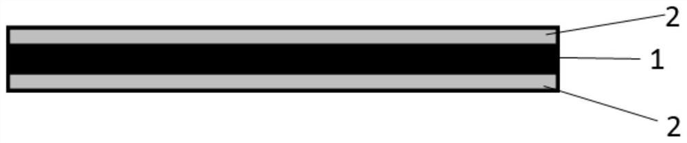
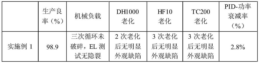
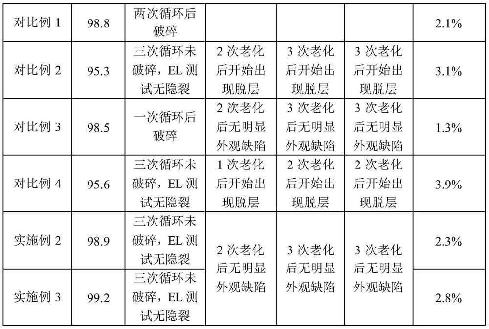
[0024] An encapsulation film structure for high-reliability photovoltaic modules, the schematic diagram of which is shown in figure 1 As shown, it consists of two non-crosslinked layers 2 and a crosslinked interlayer 1 located in the middle of the non-crosslinked layer 2;
[0025] The material of the non-crosslinked layer 2 used in the two surfaces is a non-crosslinked polymer material, the material of the crosslinked interlayer 1 in the middle is a crosslinked polymer material, and the two surface layers are non-crosslinked POE ( Provided by Andy New Materials, the model is ADSP0012 non-cross-linked POE film), the middle is cross-linked POE (provided by Andy New Materials, model is ADSP0225 cross-linked POE film), according to non-cross-linked type / cross-linked / non-cross-linked in order to prepare the multi-layer adhesive film by hot pressing to obtain the film packaging film structure. The total film thickness of the packaging film structure is about 500 μm. It is about 300...
Embodiment 2
[0035] An encapsulation film structure for high-reliability photovoltaic modules, which has the same structure as figure 1 Same, consisting of two non-crosslinked layers 2 and a crosslinked interlayer 1 located in the middle layer of the non-crosslinked layer 2;
[0036] The material of the non-crosslinked layer 2 used in the two surfaces is a non-crosslinked polymer material, the material of the crosslinked interlayer 1 in the middle is a crosslinked polymer material, and the two surface layers are non-crosslinked POE ( Provided by Andy New Materials, the model is ADSP0012 non-cross-linked POE film), the middle is cross-linked POE (provided by Andy New Materials, model is ADSP0225 cross-linked POE film), according to non-cross-linked type / cross-linked / non-cross-linked in order to prepare the multi-layer adhesive film by hot pressing to obtain the film packaging film structure. The total film thickness of the packaging film structure is about 500 μm. The thickness is about 25...
Embodiment 3
[0038] An encapsulation film structure for high-reliability photovoltaic modules, which has the same structure as figure 1 Same, consisting of two non-crosslinked layers 2 and a crosslinked interlayer 1 located in the middle layer of the non-crosslinked layer 2;
[0039] The material of the non-crosslinked layer 2 used in the two surfaces is a non-crosslinked polymer material, the material of the crosslinked interlayer 1 in the middle is a crosslinked polymer material, and the two surface layers are non-crosslinked POE ( Provided by Andy New Materials, the model is ADSP0012 non-cross-linked POE film), the middle is cross-linked POE (provided by Andy New Materials, model is ADSP0225 cross-linked POE film), according to non-cross-linked type / cross-linked / non-cross-linked in order to prepare the multi-layer adhesive film by hot pressing to obtain the film packaging film structure. The total film thickness of the packaging film structure is about 500 μm. It is about 200 μm thick....
PUM
 Abstract
Description
Claims
Application Information
 - R&D
- Intellectual Property
- Life Sciences
- Materials
- Tech Scout
- Unparalleled Data Quality
- Higher Quality Content
- 60% Fewer Hallucinations
Browse by: Latest US Patents, China's latest patents, Technical Efficacy Thesaurus, Application Domain, Technology Topic, Popular Technical Reports.
© 2025 PatSnap. All rights reserved.Legal|Privacy policy|Modern Slavery Act Transparency Statement|Sitemap|About US| Contact US: help@patsnap.com