Method for preparing N-polarity GaN based on CMP, N-polarity GaN and application of N-polarity GaN

A polarity and polarity surface technology, applied in the field of electronic science, can solve the problems of slow dry etching technology, increase of ohmic contact resistance, increase of surface roughness, etc., achieve low cost, reduce ohmic contact resistance, Effect of High Thinning Rate

Pending Publication Date: 2022-02-08
SUZHOU INST OF NANO TECH & NANO BIONICS CHINESE ACEDEMY OF SCI
View PDF0 Cites 1 Cited by
  • Summary
  • Abstract
  • Description
  • Claims
  • Application Information

AI Technical Summary

Problems solved by technology

[0008] However, the existing common dry etching technology has etching damage, which can be manifested as increased surface roughness, increased film defects, and increased ohmic contact resistance, while the low-damage dry etching technology is extremely slow. (calculated at 1nm / min, it takes 33h to etch to reduce the thickness of 2μm), resulting in extremely high cost

Method used


Image

  • Method for preparing N-polarity GaN based on CMP, N-polarity GaN and application of N-polarity GaN
  • Method for preparing N-polarity GaN based on CMP, N-polarity GaN and application of N-polarity GaN
  • Method for preparing N-polarity GaN based on CMP, N-polarity GaN and application of N-polarity GaN

Examples


Embodiment 1

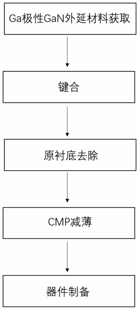
[0069] A method for preparing N-polar GaN based on CMP, comprising:

[0070] SiO with KOH as pH regulator and particle size of 10-60nm 2 As polishing abrasive particles, a polishing solution with pH=10 is configured;

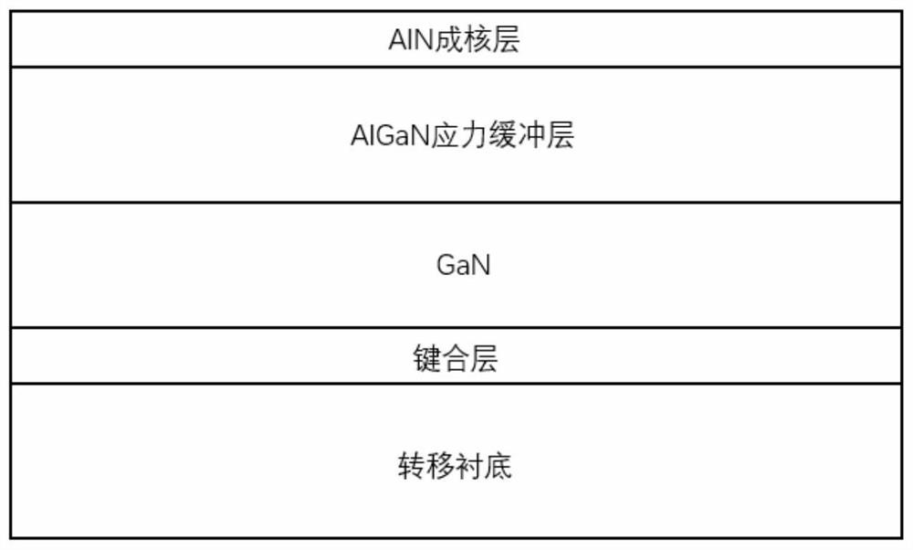
[0071] Fix the wafer to be polished and thinned in the middle of the wafer carrier, and the wafer carrier is installed on the carrier assembly, so that the surface of the wafer to be polished and thinned is in contact with the polishing pad, and the wafer to be polished and thinned is provided with 8N by the carrier assembly. The pressure, the speed of the polishing pad is 30 rpm, the flow rate of the polishing solution is 10ml / min, the speed of the wafer carrier is 50 rpm, and the polishing time is 10 minutes; use N-polar AlN (AlGaN) and N-polar GaN polishing Selective polishing with high selectivity ratio of thinning rate, fast removal of 200nm AlN nucleation layer and 2μm AlGaN stress buffer layer, slow removal of GaN layer, until the surface of N-polar GaN ...

Embodiment 2

[0074] A method for preparing N-polar GaN based on CMP, comprising:

[0075] SiO with a particle size of 20-30nm using NaOH as a pH regulator 2 As polishing abrasive particles, a polishing solution with pH=12 is configured;

[0076] Fix the wafer to be polished and thinned in the middle of the wafer carrier, and the wafer carrier is installed on the carrier assembly so that the surface of the wafer to be polished and thinned is in contact with the polishing pad; and the wafer to be polished and thinned is provided with a pressure of 15N by the carrier assembly , the rotating speed of the polishing pad is 20 rpm, the flow rate of the polishing liquid is 10ml / min, the rotating speed of the wafer carrier is 30 rpm, and the polishing time is 6 minutes; using N-polarity AlN (AlGaN) and N-polarity GaN polishing thinning Selective polishing with a high selectivity ratio, quickly removes the 200nm AlN nucleation layer and 2μm AlGaN stress buffer layer, and slowly removes the GaN laye...


PUM

PropertyMeasurementUnit
particle diameteraaaaaaaaaa
surface roughnessaaaaaaaaaa

Abstract

The invention discloses a method for preparing N-polarity GaN based on CMP, the N-polarity GaN and application of the N-polarity GaN. The method for preparing N-polarity GaN based on CMP comprises the steps of exposing an N-polarity surface of a Ga-polarity GaN material; and chemically and mechanically polishing and thinning the N-polarity surface of the Ga-polarity GaN material by adopting an alkaline polishing solution so as to expose N-polarity GaN in the Ga-polarity GaN material, wherein the alkaline polishing solution contains grinding and polishing nanoparticles. The N-polarity GaN prepared by the method for preparing the N-polarity GaN based on the CMP provided by the embodiment of the invention has no etching damage, the ohmic contact resistance can be reduced, the performance of the N-polarity GaN and the performance of a device of the N-polarity GaN are further improved, and the surface roughness of the prepared N-polarity GaN is smaller.

Description

technical field [0001] The invention particularly relates to a method for preparing N-polar GaN based on CMP, N-polar GaN and applications thereof, belonging to the field of electronic science and technology. Background technique [0002] The commonly used GaN material is a wurtzite structure. In the wurtzite GaN structure, there is no central inversion symmetry along the c-axis [0001] direction of the unit cell, so GaN materials can be divided into Ga Polar GaN material and N-polar GaN material. At present, conventional GaN materials are all prepared based on Ga-polar GaN materials. Compared with conventional Ga-polar GaN, N-polar GaN materials have completely opposite polarity, so they have many novel characteristics. [0003] Using other properties of N-polar GaN materials will have great advantages in the preparation of optoelectronic devices, detectors, switching devices and radio frequency devices. In the field of LED applications, the polarization electric field dir...

Claims


Application Information

Patent Timeline
Patent Type & Authority Applications(China)
IPC IPC(8): H01L21/306H01L33/00H01L21/335H01L29/20H01L29/778H01L33/02
CPCH01L21/30625H01L33/007H01L33/02H01L29/66462H01L29/2003H01L29/778
Inventor 张丽于子呈于国浩张宝顺
Owner SUZHOU INST OF NANO TECH & NANO BIONICS CHINESE ACEDEMY OF SCI
Why Eureka
Try Eureka