

Cleaning process for solving patterning collapse of advanced node
A patterning and node technology, applied in electrical components, semiconductor/solid-state device manufacturing, circuits, etc., can solve the problems of ineffective cleaning methods and drying processes, production process influence, patterned structure collapse, etc., to avoid The effect of graphical collapse of tension drawing
Pending Publication Date: 2022-02-11
ULTRON SEMICON (SHANGHAI) CO LTD
View PDF0 Cites 0 Cited by
- Summary
- Abstract
- Description
- Claims
- Application Information
AI Technical Summary
Problems solved by technology
[0002] The continuous advancement of wafer manufacturing technology involves the patterned structure of related nanoscale microstructures such as logic integrated circuits, storage, and micro-electromechanical systems. The size of the gate structure is continuously reduced, and the process node has changed from the popular 28nm Advance to below 5nm, on the relevant electronic channel structure on the semiconductor wafer, particles or other related pollutant residues will affect the production process, but in various cleaning, etching, deglue, film removal and electroplating of the wafer , grinding or multiple, wet processes will face the issue of removing particles and pollutants. Traditional cleaning methods and drying processes are no longer effective. The manufacturing problems that tend to be nano-scale or even close to the picometer-scale structure, in the traditional The wet-related process of the current advanced node process faces the problem of collapse of the patterned structure due to tension problems
Method used
View moreImage
Smart ImageViewing Examples

Examples
Embodiment approach
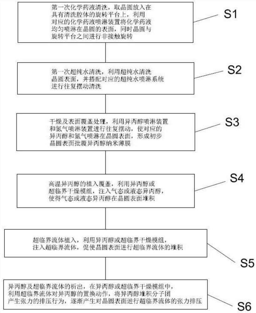
[0040] Further, as a preferred embodiment, during the first cleaning process of the chemical liquid, nitrogen gas can be passed through, and the chemical liquid can be subjected to sonic vibration and nitrogen jet flow so that the chemical liquid molecules can be finely After chemical treatment, the refined chemical liquid molecules can be more evenly distributed on the surface of the wafer under the action of nitrogen gas, which can effectively improve the cleaning effect. Secondly, the chemical liquid can be heated and degassed, which can maintain the stability of the chemical liquid and improve the cleaning efficiency.
Login to View More PUM
 Abstract
The invention discloses a cleaning process for solving patterning collapse of an advanced node, and relates to the technical field of semiconductor manufacturing. The cleaning process comprises the operation steps of first-time chemical solution cleaning, first-time ultrapure water cleaning, drying and surface covering treatment, high-temperature isopropanol implantation covering, supercritical fluid implantation, isopropanol and supercritical fluid precipitation and the like. Isopropanol molecules carrying water molecules can be removed from the surface of the wafer, so that the stability of the surface property of the wafer treated by a wet process is controlled, and the phenomenon of tension drawing graphical collapse of the water molecules and the isopropanol molecules on the surface of the wafer is avoided.
Description
technical field [0001] The invention relates to the technical field of semiconductor manufacturing, in particular to a cleaning process for solving pattern collapse of advanced nodes. Background technique [0002] The continuous advancement of wafer manufacturing technology involves the patterned structure of related nanoscale microstructures such as logic integrated circuits, storage, and micro-electromechanical systems. The size of the gate structure is continuously reduced, and the process node has changed from the popular 28nm Advance to below 5nm, on the relevant electronic channel structure on the semiconductor wafer, particles or other related pollutant residues will affect the production process, but in the various cleaning, etching, deglue, film removal, electroplating of the wafer , grinding or multiple, wet processes will face the issue of removing particles and pollutants. Traditional cleaning methods and drying processes are no longer effective. The manufacturin...
Claims
Login to View More Application Information
Patent Timeline
 Patent Type & AuthorityApplications(China)
IPC IPC(8): H01L21/02H01L21/67
CPCH01L21/02041H01L21/02101H01L21/6704H01L21/67034
Inventor廖世保刘大威卢证凯陈新来
OwnerULTRON SEMICON (SHANGHAI) CO LTD