Semiconductor power device and preparation method thereof

A power device and semiconductor technology, applied in the field of semiconductor power devices and their preparation, can solve the problems of SGTMOS incompatibility, high manufacturing cost, and difficulty in integration, and achieve the effects of easy integration, easy process compatibility, and reduced on-resistance

Pending Publication Date: 2022-02-11
江苏格瑞宝电子有限公司
View PDF0 Cites 5 Cited by
  • Summary
  • Abstract
  • Description
  • Claims
  • Application Information

AI Technical Summary

Problems solved by technology

However, the disadvantage is that the process is complex and the manufacturing cost is high; its vertical structure makes it difficult for SGT MOS to be compatible with CMOS process, so it is not easy to integrate. See the SGT structure figure 2

Method used


Image

  • Semiconductor power device and preparation method thereof
  • Semiconductor power device and preparation method thereof
  • Semiconductor power device and preparation method thereof

Examples


Embodiment 1

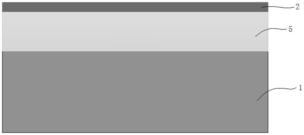
[0055] Taking NMOS as an example, a semiconductor power device of the present invention includes a substrate 1, an oxide layer 2, a dielectric layer 3, a well region 4, a drift region 5, a trench 6, a gate oxide layer 7, a field oxide layer 8, and polysilicon 9 , source 10, gate 11, drain 12, lightly doped region 13 and heavily doped region 14, wherein the substrate 1 is a P-type substrate, the well region 4 is a P-type well region, and the drift region 5 is an N-type In the drift region, N-type ions are implanted into the bottom of the trench 6 to form a lightly doped region 13 , and the upper surfaces of the well region 4 and the drift region 5 are implanted with N-type ions to form a heavily doped region 14 .

[0056] In the present invention, the substrate 1, the oxide layer 2 and the dielectric layer 3 are sequentially arranged from bottom to top, and the ion implantation in the upper surface of the P-type substrate forms a P-type well region, and the ion implantation in t...

Embodiment 2

[0074] Taking PMOS as an example, a semiconductor power device of the present invention includes a substrate 1, an oxide layer 2, a dielectric layer 3, a well region 4, a drift region 5, a trench 6, a gate oxide layer 7, a field oxide layer 8, and polysilicon 9 , source 10, gate 11, drain 12, lightly doped region 13 and heavily doped region 14, wherein the substrate 1 is an N-type substrate, the well region 4 is an N-type well region, and the drift region 5 is a P-type In the drift region, P-type ions are implanted into the bottom of the trench 6 to form a lightly doped region 13 , and P-type ions are implanted into the upper surface of the well region 4 and the drift region 5 to form a heavily doped region 14 .

[0075] In the present invention, the substrate 1, the oxide layer 2 and the dielectric layer 3 are sequentially arranged from bottom to top, and the ion implantation in the upper surface of the N-type substrate forms an N-type well region, and the ion implantation in ...


PUM


Abstract

The invention discloses a semiconductor power device and a preparation method thereof. The device comprises a substrate, an oxide layer and a dielectric layer which are sequentially arranged from bottom to top, well regions and drift regions which are arranged at intervals are formed in the upper surface of the substrate through ion implantation, a groove is formed between the adjacent well region and drift region, and a gate oxide layer is arranged on the inner side, close to the well region, of the groove. The rest inner sides of the trench are provided with field oxide layers, and the inner sides of the gate oxide layer and the field oxide layers are filled with polycrystalline silicon flush with the surface of the substrate. The advantages of the LDMOS and the SGT are combined, low on-resistance, high voltage resistance, easy integration and small occupied chip area are realized, and the semiconductor power device can be applied to the technical field of BCD.

Description

technical field [0001] The invention relates to a semiconductor device, in particular to a semiconductor power device and a preparation method thereof. Background technique [0002] Semiconductor power devices can be divided into lateral conduction power devices and vertical conduction power devices according to the structure; lateral power devices are mainly LDMOS (Laterally-diffused metal-oxide semiconductor), and vertical power devices are mainly VDMOS (Vertical-diffused metal-oxide semiconductor). semiconductor), SGT MOS (shield gatetrench or splitgatetrench MOS), IGBT (Insulated Gate Bipolar Transistor: insulated gate bipolar transistor) mainly. Semiconductor power devices are always pursuing higher withstand voltage, lower on-resistance per unit area, and reduced chip area. [0003] The advantage of LDMOS is that it is easy to integrate, compatible with CMOS technology, and widely used in BCD technology. Its shortcomings are also obvious. To obtain a higher breakdown...

Claims


Application Information

Patent Timeline
Patent Type & Authority Applications(China)
IPC IPC(8): H01L29/78H01L29/423H01L29/06H01L21/336
CPCH01L29/7809H01L29/7813H01L29/4236H01L29/0619H01L29/66734
Inventor 代萌
Owner 江苏格瑞宝电子有限公司
Why Eureka
Try Eureka