Chip bonding pad ball mounting leveling and secondary welding method

A chip pad and secondary soldering technology, which is applied in the direction of electrical components, electrical solid devices, circuits, etc., can solve the problems of poor bonding strength consistency, low bonding strength, fishtail warping, etc., and improve the strength and reliability , Improve consistency, high welding strength effect

Pending Publication Date: 2022-02-15
XIAN MICROELECTRONICS TECH INST
View PDF0 Cites 2 Cited by
  • Summary
  • Abstract
  • Description
  • Claims
  • Application Information

AI Technical Summary

Problems solved by technology

[0005] Aiming at the problems of poor welding process stability, fish tail warping, low bonding strength, and poor consistency of bonding strength caused by the top shape of the pointed cap-shaped solder ball in the existing secondary bonding method of the chip pad, the present invention provides a Chip pad ball planting leveling and secondary welding method

Method used

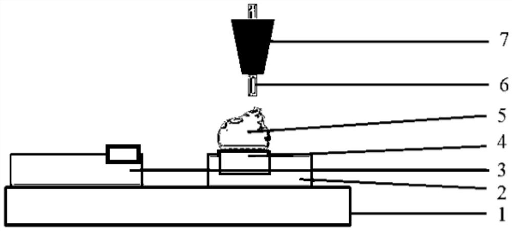
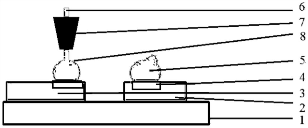
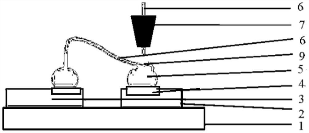

Image

  • Chip bonding pad ball mounting leveling and secondary welding method
  • Chip bonding pad ball mounting leveling and secondary welding method
  • Chip bonding pad ball mounting leveling and secondary welding method

Examples


Embodiment Construction

[0032] The present invention will be further described in detail below in conjunction with specific embodiments, which are explanations of the present invention rather than limitations.

[0033] In order to enable those skilled in the art to better understand the solutions of the present invention, the technical solutions in the embodiments of the present invention will be clearly and completely described below in conjunction with the drawings in the embodiments of the present invention. Obviously, the described embodiments are only It is an embodiment of a part of the present invention, but not all embodiments. Based on the embodiments of the present invention, all other embodiments obtained by persons of ordinary skill in the art without making creative efforts shall fall within the protection scope of the present invention.

[0034] It should be noted that the terms "first" and "second" in the description and claims of the present invention and the above drawings are used t...


PUM


Abstract

The invention provides a chip bonding pad ball-mounting leveling and secondary welding method, and the method achieves the fishtail bonding of a lead and a flat interface at the top end of a ball-mounting during secondary welding through introducing a ball-mounting shaping process. According to the method, the welding process sequence for secondary welding of a plurality of chip bonding pads in the prior art is changed, the process sequence of centralized ball mounting, centralized sharp-cap-shaped welding ball flattening and shaping and centralized secondary welding is adopted, the consistency of ball mounting morphology is improved, and the stability of the secondary welding process is improved. Aiming at an electronic device adopting a chip bonding pad secondary welding process, the consistency in the welding process is improved, the abnormities of fishtail wire warping, wire shrinkage after fishtail bonding and the like in the welding process are reduced, and the strength reliability of chip bonding pad secondary welding is improved. The method has the advantages of high yield, high efficiency, high welding strength and the like under the conditions of multi-chip interconnection, laminated chip interconnection, reverse welding of the frame carrier and the chips under the condition of complex wiring and the like.

Description

technical field [0001] The invention belongs to the field of packaging and testing of semiconductor integrated circuits, and in particular relates to a method for ball planting and leveling of chip pads and secondary welding Background technique [0002] Secondary soldering of chip pads is a common process in the field of integrated circuit packaging. It is suitable for pad soldering interconnection between chips and chips, and reverse soldering interconnection between frame carrier / substrate and chip pads. In multi-chip packaging , stacked chip packaging, high and low arc wiring packaging, etc. are widely used. Using this process can solve the problems of fishtail bonding damaged pads and too narrow line arc spacing in one welding. The main feature of this process is that some chip pads are used as secondary solder joints to carry fishtail bonding. [0003] At present, the method used for the secondary soldering of the existing chip pads is: to plant balls on the chip pad...

Claims


Application Information

Patent Timeline
Patent Type & Authority Applications(China)
IPC IPC(8): H01L23/48H01L21/60
CPCH01L24/11H01L24/81H01L2224/1111H01L2224/118H01L2224/81986H01L2224/81047
Inventor 周少明张波方兆国
Owner XIAN MICROELECTRONICS TECH INST
Why Eureka
Try Eureka