Preparation method of lead bonding interface transmission electron microscope sample and method for observing evolution process of intermetallic compound
An electron microscope and wire bonding technology, which is applied in the preparation, sampling, and measuring devices of test samples, can solve problems such as increased research errors, poor repeatability of experimental conclusions, and deviations
- Summary
- Abstract
- Description
- Claims
- Application Information
AI Technical Summary
Problems solved by technology
Method used
Image
Examples
preparation example Construction
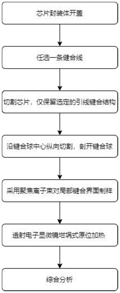
[0028] The invention provides a method for preparing a wire bonding interface transmission electron microscope sample, comprising the following steps:
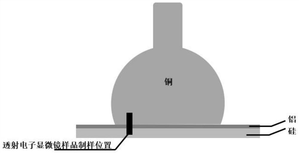
[0029] (1) Select a bonding wire from the chip wiring structure contained in the chip package, and deposit a metal protective layer on the surface of the bonding ball at one end of the bonding wire and the surface of the pad in contact with the bonding ball to obtain protected bonding balls and pads, the chip package containing a wire bonding structure;
[0030] (2) cutting the protected bonding ball and pad by ion beam to obtain bonding ball-pad sample;
[0031] (3) Cutting the bonding ball-pad sample longitudinally with an ion beam to obtain a bonding ball-pad sample with an exposed wire bonding interface;
[0032] (4) Depositing a metal protective layer on the wire bonding interface region of the bonding ball-pad sample of the exposed wire bonding interface to obtain a protected wire bonding interface;
[0033] (5) Cuttin...
Embodiment 1
[0074] (1) Select a chip package including a copper-aluminum wire bonding structure, unpack the chip, and remove the package shell.
[0075] (2) Put the chip obtained in step (1) without the package shell into the instrument of the double-beam focused ion beam-scanning electron microscope, observe the internal wiring structure of the chip from the window of the scanning electron microscope, and select a copper bond arbitrarily fit line.
[0076] (3) In step (2), select the bonding ball structure at one end of the copper bonding wire and deposit a layer of Pt protection on the surface of the surrounding pads, with a thickness of 1 μm, and use focused ion beams to dig trenches on both sides of the Pt protection layer Obtain a rough cut bond ball-pad sample from one end of the selected bond wire.
[0077] (4) The bonding ball-pad sample prepared in step (3) was longitudinally sliced to the center position, and the bonding ball sample was divided into two to obtain a bonding ba...
PUM
| Property | Measurement | Unit |
|---|---|---|
| Thickness | aaaaa | aaaaa |
| Thickness | aaaaa | aaaaa |
Abstract
Description
Claims
Application Information
 - R&D Engineer
- R&D Manager
- IP Professional
- Industry Leading Data Capabilities
- Powerful AI technology
- Patent DNA Extraction
Browse by: Latest US Patents, China's latest patents, Technical Efficacy Thesaurus, Application Domain, Technology Topic, Popular Technical Reports.
© 2024 PatSnap. All rights reserved.Legal|Privacy policy|Modern Slavery Act Transparency Statement|Sitemap|About US| Contact US: help@patsnap.com


