Semiconductor structure and manufacturing method thereof

A manufacturing method and semiconductor technology, applied in semiconductor/solid-state device manufacturing, semiconductor devices, transistors, etc., can solve problems such as high performance, underlying substrate consumption, film layer shedding, etc., achieve good electrical performance, inhibit substrate oxidation, The effect of good structural integrity

Pending Publication Date: 2022-02-18
CHANGXIN MEMORY TECH INC
View PDF0 Cites 0 Cited by
  • Summary
  • Abstract
  • Description
  • Claims
  • Application Information

AI Technical Summary

Problems solved by technology

[0002] With the shrinking of the size of semiconductor structures, the additional consumption of film materials may lead to large performance defects in the process of fabricating semiconductor structures
[0003] Specifically, a semiconductor structure usually includes an array area and a peripheral area surrounding the array area. When the underlying substrate of the array area and the peripheral area is etched and cleaned, the underlying substrate will be partially consumed or even film layers will fall off. , the consumption of substrate material will lead to performance defects of the substrate, such as leakage, etc.

Method used


Image

  • Semiconductor structure and manufacturing method thereof
  • Semiconductor structure and manufacturing method thereof
  • Semiconductor structure and manufacturing method thereof

Examples


Embodiment Construction

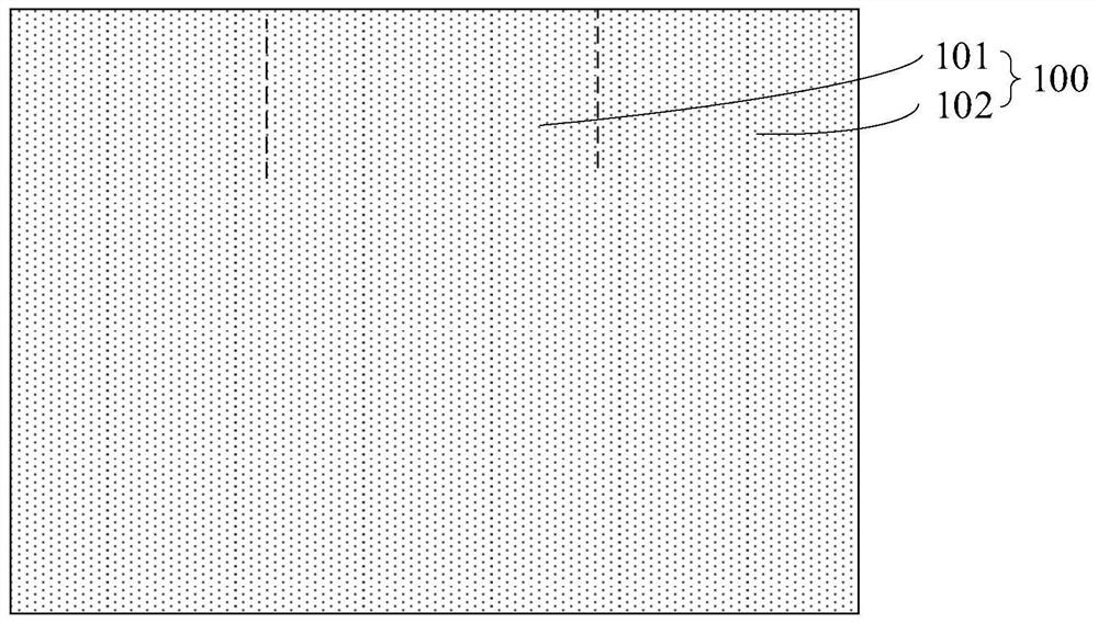
[0023] refer to figure 1 , a substrate 100 is provided, the substrate 100 includes an active region 101 and an isolation region 102 located between adjacent active regions 101 , the active region 101 includes a corner region adjacent to the isolation region 102 .

[0024] The material of the substrate 100 includes polysilicon, and the subsequent removal process for the substrate 100 is mostly performed in an atmospheric environment, where polysilicon will naturally oxidize.

[0025] It should be noted that the dividing line used to divide the active region 101 and the isolation region 102 in the illustration herein is only used for illustration. In fact, the dividing line is not necessarily perpendicular to the surface of the substrate 100, and the dividing line may also have a certain inclination angle. , the inclination angle of the dividing line may be equal to the inclination angle of the sidewall of the trench formed by subsequent etching.

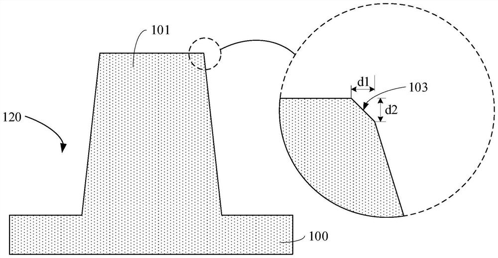
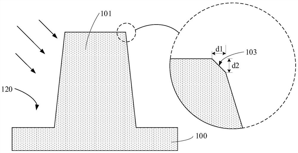
[0026] refer to figure 2 ,...


PUM


Abstract

The embodiment of the invention provides a semiconductor structure and a manufacturing method thereof, and the manufacturing method of the semiconductor structure comprises the steps of providing a substrate which comprises active regions and isolation regions located between the adjacent active regions, and the active regions comprise corner regions adjacent to the isolation regions; performing a doping process, injecting doping ions into the corner area, where the doping ions are used for slowing down the oxidation rate of the corner area; and after the doping process is carried out, performing a removal process on the substrate, where the oxidized substrate can be removed through the removal process, and in the process of carrying out the removal process, the structures in the isolation regions expose the side walls of the corner regions. The structure integrity of the corner area of the active area can be maintained.

Description

technical field [0001] Embodiments of the present invention relate to the field of semiconductors, and in particular to a semiconductor structure and a manufacturing method thereof. Background technique [0002] With the shrinking of the size of semiconductor structures, the extra consumption of film layer materials may lead to large performance defects in the process of fabricating semiconductor structures. [0003] Specifically, a semiconductor structure usually includes an array area and a peripheral area surrounding the array area. When the underlying substrate of the array area and the peripheral area is etched and cleaned, the underlying substrate will be partially consumed or even the film layer will fall off. , the consumption of the substrate material will lead to performance defects of the substrate, such as leakage and so on. Contents of the invention [0004] Embodiments of the present invention provide a semiconductor structure and a method for forming the sa...

Claims


Application Information

Patent Timeline
IPC IPC(8): H01L21/8234H01L21/265H01L21/266H01L27/088H01L29/06H01L29/36
CPCH01L21/8234H01L21/823481H01L21/26506H01L21/266H01L27/088H01L29/36H01L29/0607H01L29/0684H01L21/265H01L29/06H01L21/762
Inventor 朱柄宇洪海涵卢经文
Owner CHANGXIN MEMORY TECH INC
Why Eureka
Try Eureka