Terminal structure, package, and method for manufacturing terminal structure
A manufacturing method and structure technology, applied in the field of terminal structure, can solve problems such as deterioration of bonding strength between metallized layers and lead terminals, and achieve the effect of improving bonding strength
- Summary
- Abstract
- Description
- Claims
- Application Information
AI Technical Summary
Problems solved by technology
Method used
Image

Examples
Embodiment approach 1
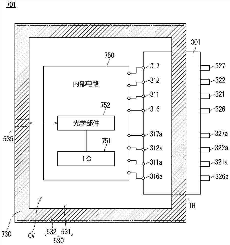
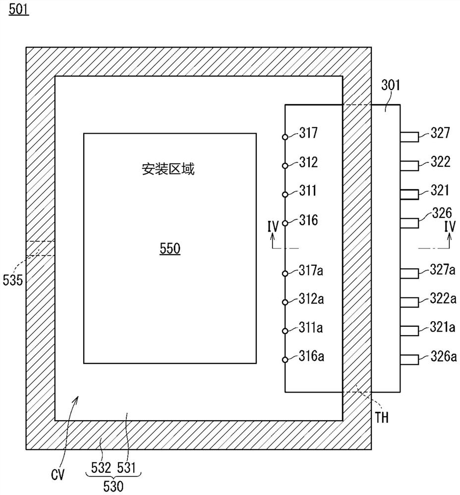
[0051] figure 1 It is a plan view schematically showing the configuration of the high-frequency module 701 in the first embodiment. In addition, about the cover body 730, only the outer edge is shown by the dashed-two dotted line for easy observation of a figure. figure 2 It is a plan view schematically showing the structure of the package 501 for obtaining the high-frequency module 701 .
[0052] High frequency module 701 ( figure 1) has a package body 501 ( figure 2 ), the cover 730 and the internal circuit 750. The internal circuit 750 has an IC (Integrated Circuit) 751 . IC751 can have a high operating frequency, specifically, an operating frequency of 55 GHz or higher. The internal circuit 750 may also have an optical component 752, and in this case, the high-frequency module 701 and the package 501 are an optical module and an optical package, respectively. Optical component 752 is, for example, a laser diode.
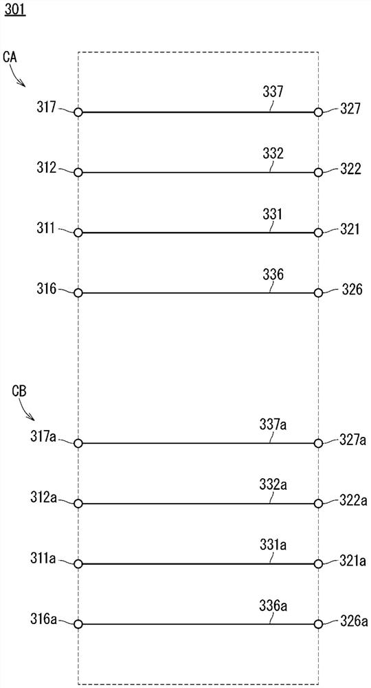
[0053] The package 501 has a terminal structure 30...
Embodiment approach 2
[0084] Figure 13 It is a partial plan view schematically showing the structure of the terminal structure 304 in the second embodiment. In this embodiment, the trench TR includes a portion between the connection layer 25 and the signal pad 21 and a portion between the connection layer 25 and the signal pad 22 . Furthermore, the signal pad 21 is completely surrounded by the edge ED and the trench TR on the main surface of the base body 10 . Specifically, the signal pad 21 has a quadrangular shape including one side constituted by the edge ED and three sides constituted by the trench TR. In addition, in Figure 13 In the example shown, the trench TR is not formed on the main surface of the base body 10 in the region in the diagonal direction from the signal pad 21 . As a modified example, the terminal structure 305 ( Figure 14 ), the trench TR is also formed on the main surface of the base body 10 in a region in the diagonal direction from the signal pad 21 .
[0085] In a...
Embodiment approach 3
[0089] Figure 15 It is a partial plan view schematically showing the configuration of the terminal structure 306 in the third embodiment. Figure 16 is along Figure 15 A schematic partial sectional view of the line XVI-XVI of .
[0090] Terminal structure 306 has signal pad 21A (first pad) and signal pad 22A (fourth pad) instead of terminal structure 301 ( Figure 6 as well as Figure 7 : The signal pad 21 and the signal pad 22 of Embodiment 1). In this embodiment, the trench TR includes the portion between the signal pad 21A and the signal pad 22A, but does not include the portion between the signal pad 21A and the ground pad 26 and the portion between the signal pad 22A and the ground pad 27. the part between. Therefore, main surface MS of base body 10 is flat between signal pad 21A and ground pad 26 and between ground pad 27 and signal pad 22A. As a result, the signal pad 21A differs from the signal pad 21 in that only one end (in the figure, the right end in contac...
PUM
| Property | Measurement | Unit |
|---|---|---|
| Thickness | aaaaa | aaaaa |
Abstract
Description
Claims
Application Information
 - R&D
- Intellectual Property
- Life Sciences
- Materials
- Tech Scout
- Unparalleled Data Quality
- Higher Quality Content
- 60% Fewer Hallucinations
Browse by: Latest US Patents, China's latest patents, Technical Efficacy Thesaurus, Application Domain, Technology Topic, Popular Technical Reports.
© 2025 PatSnap. All rights reserved.Legal|Privacy policy|Modern Slavery Act Transparency Statement|Sitemap|About US| Contact US: help@patsnap.com