
PCB board manufacturing process for 5g base station communication

A technology for PCB board, base station communication, applied in the directions of printed circuit manufacturing, printed circuit, electrical components, etc., can solve the problem of reducing the communication quality and fault tolerance rate of the PCB board, reducing the stability of the protective communication work of the PCB board, increasing the weight of the PCB board and Volume and other issues, to avoid loosening and dislocation of components, increase protection and heat dissipation, improve convenience and work efficiency

Active Publication Date: 2022-07-29
XINFENG FUCHANGFA ELECTRONICS
View PDF12 Cites 0 Cited by
  • Summary
  • Abstract
  • Description
  • Claims
  • Application Information

AI Technical Summary

Problems solved by technology

[0003] When the current PCB board is manufactured and assembled, it is often necessary to install components such as filters, receiving antennas, and protective covers outside the board to ensure that the PCB board is placed outside for communication. However, due to the higher integration of the configured components, the structure It is relatively complicated, which increases the weight and volume of the PCB board, and increases the difficulty factor of the overall assembly of the base station, and the PCB board may be subjected to vibration and shock caused by human or external objects during production, assembly and actual use, so that the PCB board Loose or misplaced components will reduce the protection of the PCB board and the stability of communication work. In addition, during the communication period of the PCB board, it may be interfered by external signals, resulting in too slow signal processing efficiency of the PCB board or incomplete reception of information. When the PCB board is in operation, it will generate a lot of heat. This heat is easy to concentrate on the surface of the circuit board, which is difficult to discharge from the disk, and reduces the communication quality and fault tolerance rate of the PCB board.

Method used


Image

  • PCB board manufacturing process for 5g base station communication
  • PCB board manufacturing process for 5g base station communication
  • PCB board manufacturing process for 5g base station communication

Examples


Embodiment 1

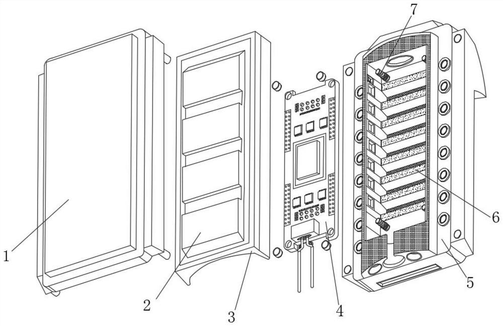
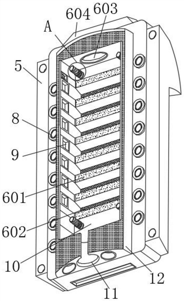
[0044] Example 1, as Figure 3-4 As shown, when the PCB board body 4 is assembled inside the groove 10, the PCB board body 4 can be inserted into the positioning bolts 703 through the positioning holes 702 opened, and the PCB board body 4 is urged to be attached to the spring 704, and then the PCB board body 4 can pass through The nut 701 fixes the positioning bolt 703 by thread, but does not lock the PCB body 4 to the maximum extent, so that the PCB body 4 can be stretched and moved under the elastic contact of the spring 704, so as to avoid the impact and vibration on the device directly acting on the PCB body 4 surfaces, providing the protection of the PCB body 4 and the stability of the communication operation.

Embodiment 2

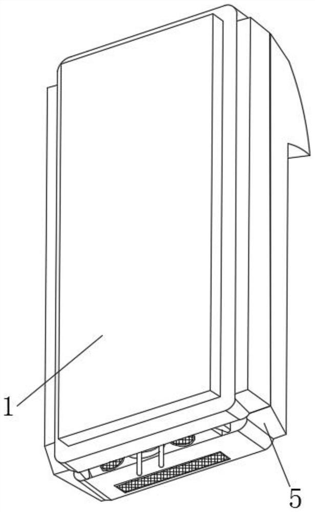
[0045] Example 2, as Figure 1-5 As shown, when the PCB board is assembled and assembled, the antenna board 2 and the arc filter board 3 can be inserted into the inner side of the fixed protective cover 1 to form an integration, and the protective cover 1 and the base 5 can be spliced ​​together. At this time, four sets of positioning sleeves at the four corners of the protective cover 1 are inserted into the fixing holes opened at the four corners of the base 5 for assembly, and four sets of fixing bolts are used to screw the inserted positioning sleeves, so as to connect the antenna plate 2 and the arc filter. The board 3 and the PCB board body 4 are assembled between the protective cover 1 and the base 5 respectively, which reduces the integration degree of the combined structure of the device, promotes the overall lightweight of the PCB board, and provides convenience for subsequent base station assembly operations.

[0046] Working principle: When the device is in use, th...


PUM


Abstract

The invention discloses a PCB board manufacturing process for 5G base station communication, and specifically relates to the technical field of PCB boards. The specific manufacturing steps are as follows: first, prepare raw materials for PCB board manufacturing, and then install on the surface of the base when the PCB board body is assembled as a whole The arc-shaped seat is provided with a groove suitable for the size of the PCB body on the inner side of the arc-shaped seat, so that the PCB body is installed based on the groove, and the heat dissipation graphite layer is laid on the inner side of the groove and multiple sets of shielding covers are installed. , multiple sets of magnetic rings are installed on the outer side of the arc-shaped seat; the present invention promotes the protection of the The cover and base can be directly assembled into a whole, and the internal antenna board, arc filter board and PCB board can work safely and stably, greatly simplifying the thickness and quality of the PCB board structure integration, and improving the convenience of base station assembly operations. and work efficiency.

Description

technical field [0001] The invention relates to the technical field of PCB boards, in particular to a PCB board manufacturing process for 5G base station communication. Background technique [0002] A wireless communication base station refers to a radio transceiver station that transmits information with wireless terminals through a wireless communication exchange center in a certain radio coverage area. Also known as printed circuit board, it is an important electronic component, a support body for electronic components, and a carrier for electrical interconnection of electronic components; [0003] When the current PCB board is produced and assembled, it is often necessary to set up components such as filters, receiving antennas, and protective covers outside the board to ensure that the PCB board is placed in the outside world for communication work. However, due to the higher integration of the components, the structure It is more complicated, which increases the weigh...

Claims


Application Information

Patent Timeline
Patent Type & Authority Patents(China)
IPC IPC(8): H05K3/00
CPCH05K3/00
Inventor 叶何远苏惠武赖剑锋张惠琳陈小杨
Owner XINFENG FUCHANGFA ELECTRONICS
Learn More