Eureka AIR delivers breakthrough ideas for toughest innovation challenges, trusted by R&D personnel around the world.

High-speed silicon light modulator phase shift arm and preparation method thereof

A modulator and silicon photonics technology, applied in the field of optical communication, to achieve the effect of increasing bandwidth and increasing optical loss

Pending Publication Date: 2022-03-01
FENGHUO COMM SCI & TECH CO LTD +1
View PDF0 Cites 0 Cited by
  • Summary
  • Abstract
  • Description
  • Claims
  • Application Information

AI Technical Summary

Problems solved by technology

The main physical structure based on silicon optical modulator is PN junction or PIN junction, so the doping concentration in PN junction or PIN junction determines the basic performance of silicon optical modulator, generally speaking, the doping concentration of PN junction or PIN junction The higher the PN junction or PIN junction response will be block, because high doping concentration can reduce the internal resistance of PN junction or PIN junction, improve the bandwidth of silicon light modulator, however, increase the doping of PN junction or PIN junction The concentration will cause more optical loss, and the optical loss is determined by the product of the doping concentration and the optical field intensity; therefore, new methods and technologies are needed to eliminate or alleviate the problem of the bandwidth and optical loss design contradiction of silicon optical modulators

Method used


Image

  • High-speed silicon light modulator phase shift arm and preparation method thereof
  • High-speed silicon light modulator phase shift arm and preparation method thereof
  • High-speed silicon light modulator phase shift arm and preparation method thereof

Examples


Embodiment 1

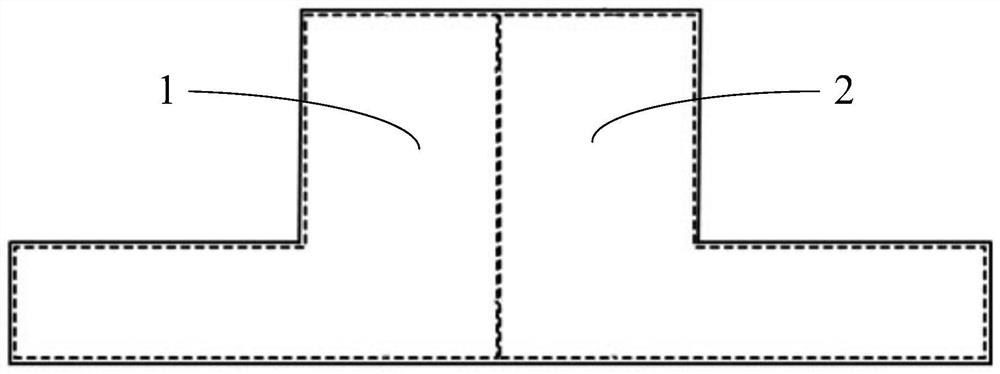
[0049] An embodiment of the present invention provides a high-speed silicon optical modulator phase shift arm, such as figure 1 As shown, it includes: a ridge waveguide; the P-type doped region and the N-type doped region are respectively located on both sides of the ridge-shaped waveguide.

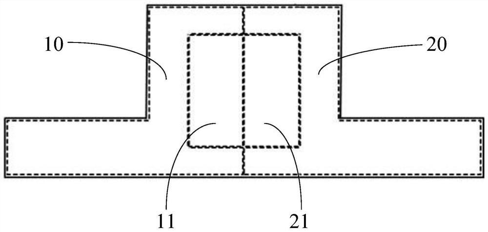
[0050] Such as figure 2 As shown, the P-type doped region includes a P-type heavily doped region and a P-type lightly doped region; the P-type heavily doped region is located at the boundary region of the ridge waveguide, and the P-type lightly doped region is located at the ridge waveguide core region of the waveguide.

[0051] The N-type doped region includes an N-type heavily doped region and an N-type lightly doped region; the N-type heavily doped region is located at the boundary region of the ridge waveguide, and the N-type lightly doped region is located at the core of the ridge waveguide area.

[0052] Wherein, the average doping concentration of the P-type heavily doped regio...

Embodiment 2

[0068] An embodiment of the present invention provides a method for preparing a phase shift arm of a high-speed silicon optical modulator. By ion implantation doping, a P-type heavily doped region and an N-type heavily doped region are arranged in the boundary region of a ridge waveguide, and a P-type The lightly doped region and the N-type lightly doped region are arranged in the core region of the ridge waveguide.

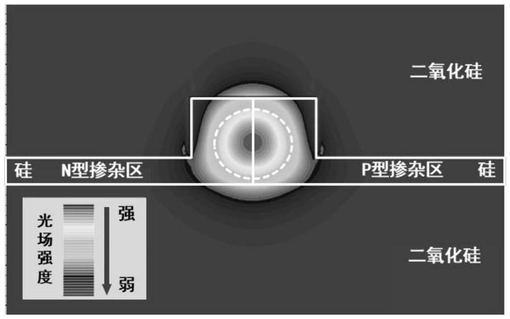
[0069] Wherein, the average doping concentration of the P-type heavily doped region is higher than the average doping concentration of the P-type lightly doped region; the average doping concentration of the N-type heavily doped region is higher than that of the N-type lightly doped region The average doping concentration of the ridge waveguide; the optical field intensity in the boundary region of the ridge waveguide is smaller than that in the core region of the ridge waveguide.

[0070] In the embodiment of the present invention, such as Figure 6 As shown, t...

Embodiment 3

[0091] The present invention provides two typical process conditions, which are used to illustrate the technical effect of the above-mentioned doping process; as Figure 7 As shown, recipe 1 is a process parameter designed for a ridge waveguide with a height of 220nm, and recipe 2 is another process parameter designed for a ridge waveguide with a height of 340nm; these two recipes are at different heights In the ridge waveguide, the doping concentration in the core region of the ridge waveguide is low and the doping concentration in the boundary region is high.

[0092] Such as Figure 7 As shown, since formula 2 is aimed at a ridge waveguide with a height of 340nm, and formula 1 is aimed at a ridge waveguide with a height of 220nm, the magnitudes of the first energy, the second energy and the third energy in formula 1 increase successively The size of the fourth energy, the fifth energy and the sixth energy in the formula 1 increases successively; the size of the first energ...


PUM


Abstract

The invention relates to the field of optical communication, and provides a high-speed silicon optical modulator phase shift arm and a preparation method thereof, and the high-speed silicon optical modulator phase shift arm comprises a ridge waveguide; the P-type doped region and the N-type doped region are located on the two sides of the ridge waveguide respectively. The P-type doped region comprises a P-type heavily doped region and a P-type lightly doped region; the P-type heavily doped region is located in a boundary region of the ridge waveguide, and the P-type lightly doped region is located in a core region of the ridge waveguide; the N-type doped region comprises an N-type heavily doped region and an N-type lightly doped region; the N-type heavily doped region is located in a boundary region of the ridge waveguide, and the N-type lightly doped region is located in a core region of the ridge waveguide; according to the invention, high-concentration ion doping is carried out in a boundary region with a relatively weak light field in the ridge-shaped waveguide, and low-concentration ion doping is carried out in a core region with a relatively strong light field in the ridge-shaped waveguide, so that the bandwidth of the silicon light modulator is improved, and meanwhile, the optical loss cannot be greatly increased.

Description

technical field [0001] The invention relates to the field of optical communication, in particular to a phase-shift arm of a high-speed silicon optical modulator and a preparation method thereof. Background technique [0002] In an optical communication system, the optical transmitting unit is an essential part, and the optical modulator is the core unit for converting electrical and optical signals. At present, optical modulators are based on three major categories of functional materials, lithium niobate, III-V compound semiconductors, and silicon materials. In terms of modulator performance, especially optoelectronic bandwidth and optical loss, lithium niobate and III-V compound semiconductor materials are significantly better than silicon materials, but silicon materials are more suitable for mass production, functional integration, and subsequent packaging The performance improvement of silicon optical modulators can bring greater economic benefits. [0003] The core o...

Claims


Application Information

Patent Timeline
IPC IPC(8): G02F1/025
CPCG02F1/025Y02P70/50
Inventor 余胜曹权
Owner FENGHUO COMM SCI & TECH CO LTD
Why Eureka
Eureka Blog
Learn More