Quantum well structure, LED chip and manufacturing method

A LED chip and quantum well technology, applied in the field of quantum well structure, can solve the problems of decreased internal quantum efficiency, poor wavelength uniformity, low thermal stability, etc., and achieve the effects of clear quality, reduced stress, and reduced separation degree

Pending Publication Date: 2022-03-08
江西乾照光电有限公司
View PDF0 Cites 2 Cited by
  • Summary
  • Abstract
  • Description
  • Claims
  • Application Information

AI Technical Summary

Problems solved by technology

However, due to the traditional multilayer quantum well In y Ga 1-y In N layer and GaN layer superlattice structure y Ga 1-y The InN thermal stability of the N layer is low, which is easy to cause InN vacancies that are thermally decomposed, thus aggravating the InN y Ga 1-y The segregation and enrichment of In in the N layer, which will cause the In y Ga 1-y Inhomogeneous stress between heterojunction materials in N-layer and GaN-layer superlattice structures, resulting in problems such as poor wavelength uniformity and decreased internal quantum efficiency

Method used


Image

  • Quantum well structure, LED chip and manufacturing method
  • Quantum well structure, LED chip and manufacturing method
  • Quantum well structure, LED chip and manufacturing method

Examples


Embodiment Construction

[0042] The following will clearly and completely describe the technical solutions in the embodiments of the present invention with reference to the accompanying drawings in the embodiments of the present invention. Obviously, the described embodiments are only some, not all, embodiments of the present invention. Based on the embodiments of the present invention, all other embodiments obtained by persons of ordinary skill in the art without making creative efforts belong to the protection scope of the present invention.

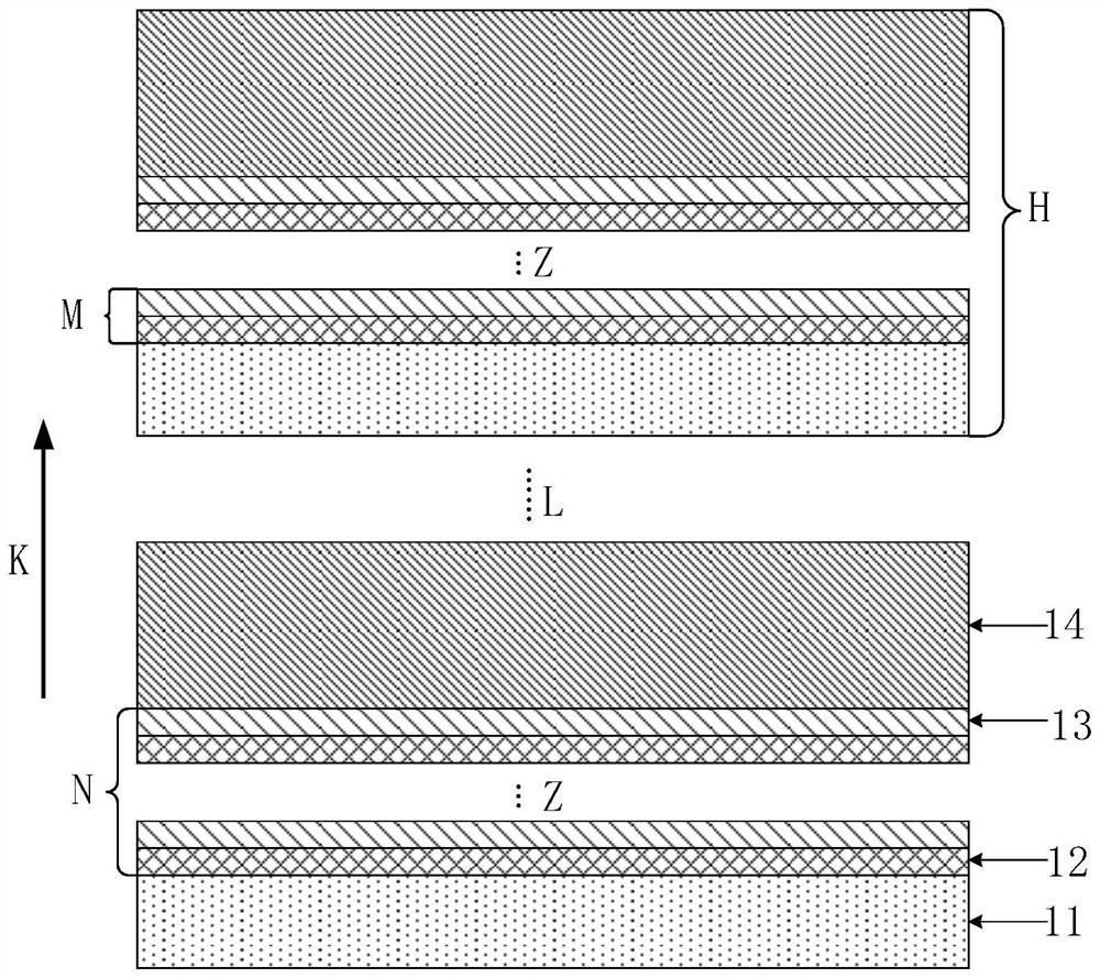
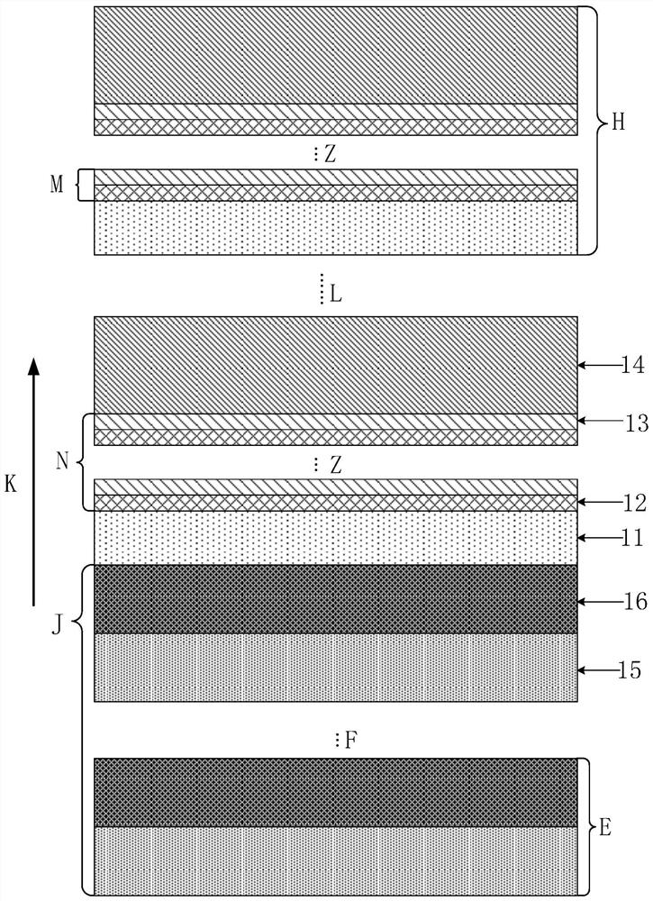
[0043] Based on the content recorded in the background technology, during the invention and creation process of the present application, the inventor found that the traditional multilayer quantum well structure is directly formed by In y Ga 1-y The composition of the N layer and the GaN layer, due to the difference in the lattice constants of the two materials, leads to the emergence of the polarization field, which leads to the bending of the energy band, and...


PUM

PropertyMeasurementUnit
thicknessaaaaaaaaaa
thicknessaaaaaaaaaa
thicknessaaaaaaaaaa

Abstract

The invention provides a quantum well structure, an LED chip and a manufacturing method, the quantum well structure comprises a plurality of quantum well laminations, each quantum well lamination comprises an In < y > Ga < 1-y > N layer, a superlattice treatment layer and a GaN layer, and each superlattice treatment layer comprises an InN layer and an In < x > Ga < 1-x > N layer. Due to the fact that the mobility of In in the InN layer and the In < x > Ga < 1-x > N layer is high, InN vacancies decomposed by heat in the In < y > Ga < 1-y > N layer of the quantum well structure can be effectively compensated, lattice defects of the In < y > Ga < 1-y > N layer can be repaired, segregation and enrichment phenomena of In in the In < y > Ga < 1-y > N layer are improved at the same time, component distribution of In is uniform, a clear interface with good quality is provided for subsequent GaN growth, and the yield of GaN is improved. And the stress generated by lattice mismatch of the InyGa1-yN layer and the GaN layer is reduced, so that the wavelength uniformity and the internal quantum efficiency are improved.

Description

technical field [0001] The invention relates to the technical field of LEDs, and more specifically relates to a quantum well structure, an LED chip and a manufacturing method. Background technique [0002] As a new type of semiconductor solid-state light source, light-emitting diode (LED) has set off a new wave in the field of lighting due to its superior performance. Especially mini-LED, because of its smaller particles, more delicate display effect, and higher brightness compared with traditional LEDs, has become a hot spot of scientific research at home and abroad. [0003] With the advancement of technology and the improvement of technology level, mini-LED has also made great breakthroughs in luminous efficiency and epitaxial growth technology. However, compared with traditional LED, mini-LED still has some problems to be solved urgently. For example, mini - LEDs have particularly high requirements for epitaxial wavelength uniformity, which is also one of the important ...

Claims


Application Information

Patent Timeline
Patent Type & Authority Applications(China)
IPC IPC(8): H01L33/06H01L33/00H01L33/12H01L33/32
CPCH01L33/06H01L33/12H01L33/007H01L33/325
Inventor 聂虎臣崔晓慧霍丽艳刘兆
Owner 江西乾照光电有限公司
Why Eureka
Try Eureka