Semiconductor material annealing device and annealing method

An annealing device, semiconductor technology, applied in the direction of polycrystalline material growth, chemical instruments and methods, metal material coating process, etc., can solve the problems of low annealing efficiency, high energy consumption, etc., and achieve the effect of simple structure and cost reduction

Pending Publication Date: 2022-03-18
ZHEJIANG UNIV HANGZHOU GLOBAL SCI & TECH INNOVATION CENT
View PDF0 Cites 0 Cited by
  • Summary
  • Abstract
  • Description
  • Claims
  • Application Information

AI Technical Summary

Problems solved by technology

[0005] Aiming at the technical problems of high energy consumption and low annealing efficiency caused by multiple heating and cooling operations of the existing annealing device in use, the present invention provides a semiconductor material annealing device and annealing method, which can realize continuous heating , without repeated heating and cooling operations, effectively reducing energy consumption and improving annealing efficiency

Method used


Image

  • Semiconductor material annealing device and annealing method
  • Semiconductor material annealing device and annealing method

Examples


Embodiment 1

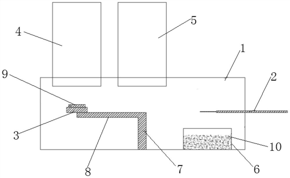
[0038] combined with Figure 1-2 , the present embodiment provides a semiconductor material annealing device, comprising: a transfer chamber 1, a sample loading platform 3 is provided in the transfer chamber 1, a sample transfer device 2 is movable on the transfer chamber 1, and the sample transfer device 2 is used for placing and removing the sample 9 on the sample loading platform 3; the first heating chamber 4, the first heating chamber 4 communicates with the transfer chamber 1, and the first heating chamber 4 is used for performing the sample 9 Pyrolysis treatment; the second heating chamber 5, the second heating chamber 5 communicates with the transfer chamber 1, the second heating chamber 5 is used to anneal the sample 9; the cooling chamber 6, the cooling chamber 6 communicates with the transfer chamber 1, the cooling chamber 6 is used to cool the sample 9 processed in the first heating chamber 4 or the second heating chamber 5; the rotating lifting mechanism, the rota...

Embodiment 2

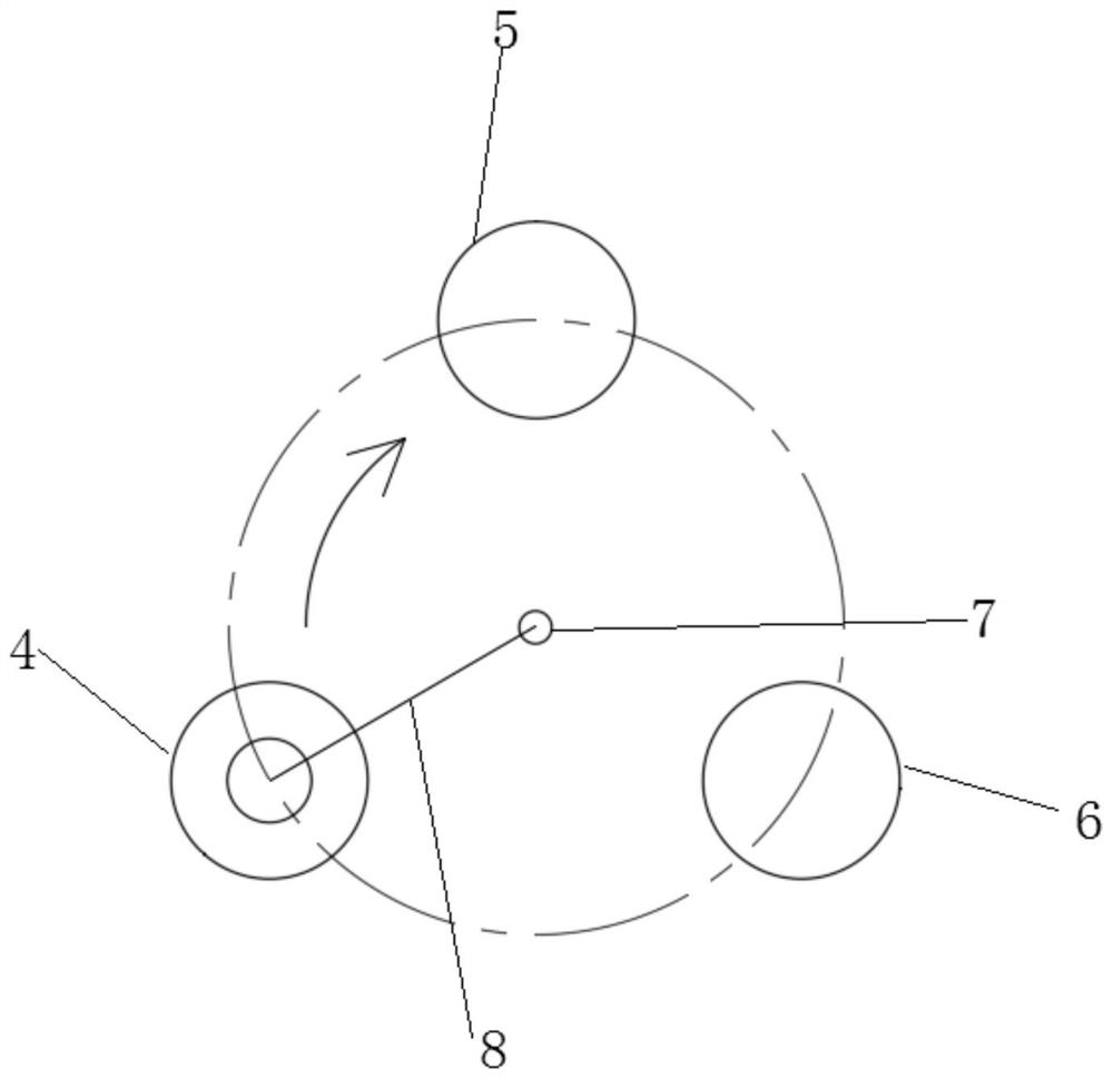
[0045] combined with figure 2 , a semiconductor material annealing device of this embodiment, compared with the technical solution of Embodiment 1, the centers of the first heating chamber 4, the second heating chamber 5 and the cooling chamber 6 are projected onto the same plane , the centers of the first heating chamber 4 , the second heating chamber 5 and the cooling chamber 6 are uniformly distributed in a manner of concentric circles.

[0046] Such as figure 2 As shown, looking down from top to bottom, the centers of the first heating chamber 4, the second heating chamber 5 and the cooling chamber 6 are projected on the same plane and evenly distributed in the form of concentric circles, so that the rotating lifting mechanism The rotation angle between the chambers can be fixed at 120°, so as to ensure the accuracy of the rotation positioning of the rotary lifting mechanism and reduce the positioning error; and this setting keeps a certain effective distance between ea...

Embodiment 3

[0048] combined with Figure 1-2 , a semiconductor material annealing device of this embodiment, compared with the technical solution of Embodiment 2, the rotary lifting mechanism includes a vertical support structure 7 and a horizontal support structure 8, and the vertical support structure 7 and the horizontal support structure The support structure 8 is vertically connected, and the vertical support structure 7 is located at the center of the concentric circle between the centers of the first heating chamber 4, the second heating chamber 5 and the cooling chamber 6, and the sample loading platform 3 is located at On the horizontal support structure 8 , and the position of the sample loading platform 3 on the horizontal support structure 8 corresponds to the center of the first heating chamber 4 , the second heating chamber 5 and the cooling chamber 6 .

[0049] Such as figure 2 As shown, looking down from top to bottom, take the position of the vertical support structure ...


PUM


Abstract

The invention discloses a semiconductor material annealing device and an annealing method, and relates to the technical field of semiconductor manufacturing, the semiconductor material annealing device comprises a transfer chamber, a sample carrying table is arranged in the transfer chamber, and a sample conveying device is movably arranged on the transfer chamber; the first heating chamber is communicated with the transfer chamber; the second heating chamber is communicated with the transfer chamber; the cooling chamber is communicated with the transfer chamber; the rotary lifting mechanism is connected with the sample carrying table, and the rotary lifting mechanism is used for driving the sample carrying table and carrying the sample to be switched among the first heating chamber, the second heating chamber and the cooling chamber. According to the annealing device, continuous heating can be achieved, repeated heating and cooling operation is not needed, energy consumption in the working process is effectively reduced, the annealing efficiency is improved, all the chambers can work in a matched mode and can also work independently, and the production cost is further reduced.

Description

technical field [0001] The invention relates to the technical field of semiconductor manufacturing, in particular to a semiconductor material annealing device and an annealing method. Background technique [0002] In the semiconductor industry, heat treatment of semiconductor materials is essential. Its main purpose is to release internal stress, increase the ductility of the material, reduce the tendency of deformation and cracks, and also change the crystal phase structure on the surface or inside of the semiconductor material. Defects, etc., to obtain the desired specific performance. In actual production, annealing treatment is one of the most commonly used methods in the heat treatment process of semiconductor materials. [0003] At present, the existing annealing device generally includes two chambers, namely a heating chamber and a cooling chamber; In order to lower the temperature of the semiconductor material after the annealing process, a transfer device is used ...

Claims


Application Information

Patent Timeline
IPC IPC(8): C30B33/02C30B29/36C23C16/26C23C16/52
CPCC30B33/02C30B29/36C23C16/26C23C16/52
Inventor 王蓉王芸霞皮孝东沈典宇杨德仁
Owner ZHEJIANG UNIV HANGZHOU GLOBAL SCI & TECH INNOVATION CENT
Why Eureka
Try Eureka