Method for forming polycrystalline structure welding spot by prefabricating IMC bonding pad

A technology of polycrystalline structure and pads, which is applied in welding media, manufacturing tools, welding equipment, etc., can solve the problems of reducing the service life and failure of electronic products, and achieve the reduction of unfavorable grain orientation, controllable solder joint size, and process simple effect

Active Publication Date: 2022-03-22
BEIJING UNIV OF TECH
View PDF7 Cites 0 Cited by
  • Summary
  • Abstract
  • Description
  • Claims
  • Application Information

AI Technical Summary

Problems solved by technology

At present, it is a thermodynamic problem to deeply understand and predict the growth mode of Sn dendrites. After the interconnection is completed, each solder joint has a unique crystal orientation, so it is inevitable that there will be some solder joints due to the growth of β-Sn grains. Unfavorable orientation, premature failure during the use of electronic products, thereby reducing the service life of electronic products

Method used


Image

  • Method for forming polycrystalline structure welding spot by prefabricating IMC bonding pad
  • Method for forming polycrystalline structure welding spot by prefabricating IMC bonding pad
  • Method for forming polycrystalline structure welding spot by prefabricating IMC bonding pad

Examples


Embodiment 1

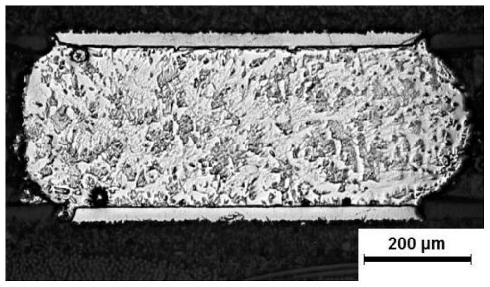
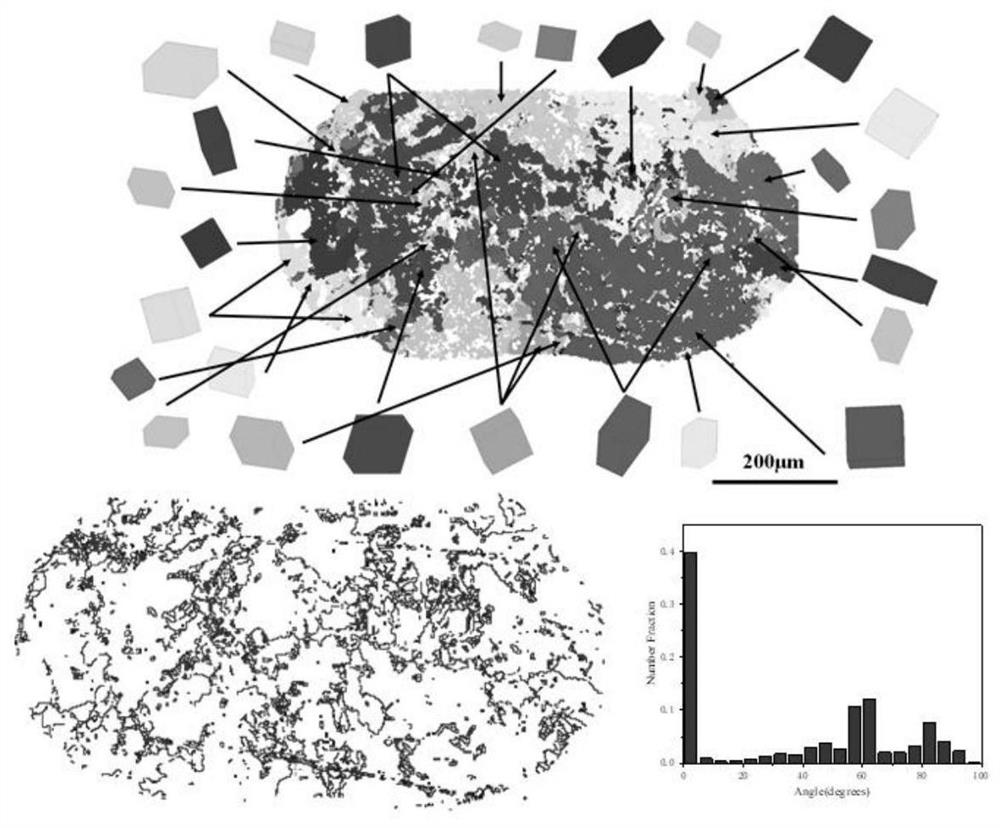
[0039] The preparation of the IMC / SABI / Cu welding spot of the polycrystalline structure of embodiment 1 different crystal orientations

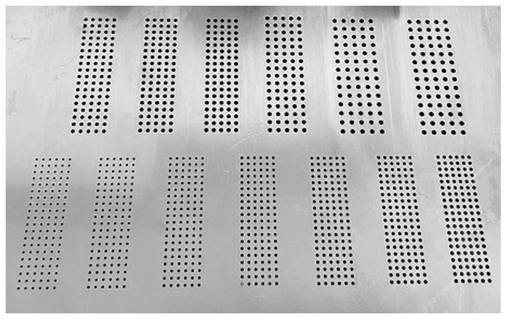
[0040] (1) The Sn-Ag-Bi-In solder is printed on the glass plate through the screen, and the size of the screen is 700 μm;

[0041] (2) Heat the missed-printed solder to form a Sn-Ag-Bi-In solder ball with a size of 700 μm by hot air soldering equipment (US PACE ST325, the same below). The remelting temperature is 245°C and the remelting time is 30s , cooling with the furnace for 30s;

[0042] (3) Use acetone and ethanol successively to clean the Sn-Ag-Bi-In solder balls in an ultrasonic cleaner;

[0043] (4) Under a stereo microscope, select Sn-Ag-Bi-In solder balls that are consistent with the pad size (700 μm) for use;

[0044] (5) Clean the surface of the PCB board with ethanol in an ultrasonic cleaner;

[0045] (6) Coat a layer of flux (ALPHA POP707, the same below) on the PCB;

[0046](7) Put the prefabricated Sn-Ag-Bi-In solder ball...

Embodiment 2

[0056] (1) The Sn-Ag-Bi-In solder is printed on the glass plate through the screen, and the size of the screen is 700 μm;

[0057] (2) Heat the missing solder by hot air soldering equipment to form Sn-Ag-Bi-In solder balls with a size of 700 μm. The remelting temperature is 245°C, the remelting time is 30s, and the furnace is cooled for 30s;

[0058] (3) Use acetone and ethanol successively to clean the Sn-Ag-Bi-In solder balls in an ultrasonic cleaner;

[0059] (4) Under a stereo microscope, select Sn-Ag-Bi-In solder balls that are consistent with the pad size (700 μm) for use;

[0060] (5) Clean the surface of the PCB board with ethanol in an ultrasonic cleaner;

[0061] (6) Coating a layer of flux on the PCB;

[0062] (7) Put the prefabricated Sn-Ag-Bi-In solder ball on the copper sheet on the surface of the PCB and heat it with hot air welding equipment to remelt the solder ball and combine it with the copper sheet on the PCB board. The remelting temperature is 200°C , ...

Embodiment 3

[0072] (1) The Sn-Ag-Bi-In solder is printed on the glass plate through the screen, and the size of the screen is 700 μm;

[0073] (2) Heat the missed-printed solder to form a Sn-Ag-Bi-In solder ball with a size of 700 μm by hot air soldering equipment (US PACE ST325, the same below). The remelting temperature is 245°C and the remelting time is 30s , cooling with the furnace for 30s;

[0074] (3) Use acetone and ethanol successively to clean the Sn-Ag-Bi-In solder balls in an ultrasonic cleaner;

[0075] (4) Under a stereo microscope, select Sn-Ag-Bi-In solder balls that are consistent with the pad size (700 μm) for use;

[0076] (5) Clean the surface of the PCB board with ethanol in an ultrasonic cleaner;

[0077] (6) Coating a layer of flux on the PCB;

[0078] (7) Put the prefabricated Sn-Ag-Bi-In solder ball on the copper sheet on the surface of the PCB and heat it with hot air welding equipment to remelt the solder ball and combine it with the copper sheet on the PCB b...


PUM


Abstract

The invention discloses a method for forming a polycrystalline structure welding spot by prefabricating an IMC bonding pad, and belongs to the technical field of material preparation and connection, the polycrystalline structure welding spot is formed by prefabricating the IMC bonding pad, and the method comprises the key steps that a welding ball is remelted and cooled on the prefabricated IMC bonding pad; the condition that the reliability and the service life of a Sn-based brazing filler metal welding spot are reduced due to anisotropy of Sn can be improved, and the welding spot is determined to be a polycrystalline structure welding spot through the EBSD technology. Therefore, the polycrystalline structure welding spots can effectively reduce the condition of unfavorable Sn grain orientation; the process is simple, the cost is low, and polycrystalline welding spots with controllable welding spot sizes and different grain orientations are manufactured.

Description

technical field [0001] The invention relates to the technical field of material preparation and connection, in particular to a method for forming polycrystalline solder joints by prefabricating IMC pads. Background technique [0002] Solder joints play the role of mechanical connection and electrical signal transmission in microelectronic interconnection. At present, the space of microelectronic packaging is reduced, the number of components is increased, and the heat generation of components is intensified; moreover, the current density that solder joints bear is constantly increasing. Driven by thermodynamic and kinetic factors, the IMCs formed in the solder will grow or dissolve, causing the failure of the solder joints, thereby affecting the service life and reliability of electronic products. At present, the solder used in microelectronic interconnection is mainly Sn-based solder (containing more than 80% Sn), and the crystal structure of Sn mainly affects the reliabili...

Claims


Application Information

Patent Timeline
Patent Type & Authority Applications(China)
IPC IPC(8): B23K1/00B23K1/20B23K3/04B23K3/08B23K35/02B23K35/28
CPCB23K1/00B23K1/206B23K1/203B23K3/04B23K3/08B23K35/0222B23K35/282
Inventor 汉晶孟洲郭福马立民晋学轮曹恒李腾贾强周炜王晓露
Owner BEIJING UNIV OF TECH
Why Eureka
Try Eureka