Display device

A technology for display devices and display panels, which is applied in the directions of identification devices, instruments, electrical components, etc., can solve the problems of bulging and wrinkling of edges and delamination of film layers, and achieves the effect of reducing costs and improving the rate of dismantling and repairing.

Pending Publication Date: 2022-03-22
WUHAN CHINA STAR OPTOELECTRONICS SEMICON DISPLAY TECH CO LTD
View PDF4 Cites 1 Cited by
  • Summary
  • Abstract
  • Description
  • Claims
  • Application Information

AI Technical Summary

Problems solved by technology

[0004] The present invention provides a display device, which can effectively solve the problems of film layer delamination and edge bulging and wrinkling in the process of dismantling and repairing the current display device

Method used


Image

  • Display device
  • Display device
  • Display device

Examples


Embodiment 1

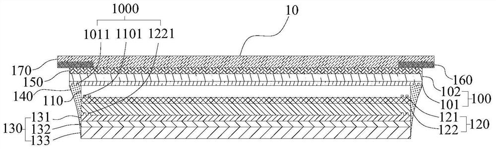
[0033] figure 1 It is a schematic structural diagram of a display device provided by Embodiment 1 of the present invention; figure 2 It is a schematic cross-sectional view of some film layers in the display device provided by Embodiment 1 of the present invention. combine figure 1 with figure 2 As shown, the present invention provides a display device 10, and the display device 10 may be a flat display device.

[0034] In this embodiment, the display device 10 includes a display panel 100, and the display panel 100 is configured to perform a display function. In this embodiment, the display panel 100 is, for example, an OLED display panel. Certainly, the present invention does not limit the type of the display panel 100 , and in other embodiments of the present application, the display panel 100 may also be a liquid crystal display panel or an inorganic light emitting diode display panel.

[0035] In this embodiment, the display panel 100 includes a base substrate 101 a...

Embodiment 2

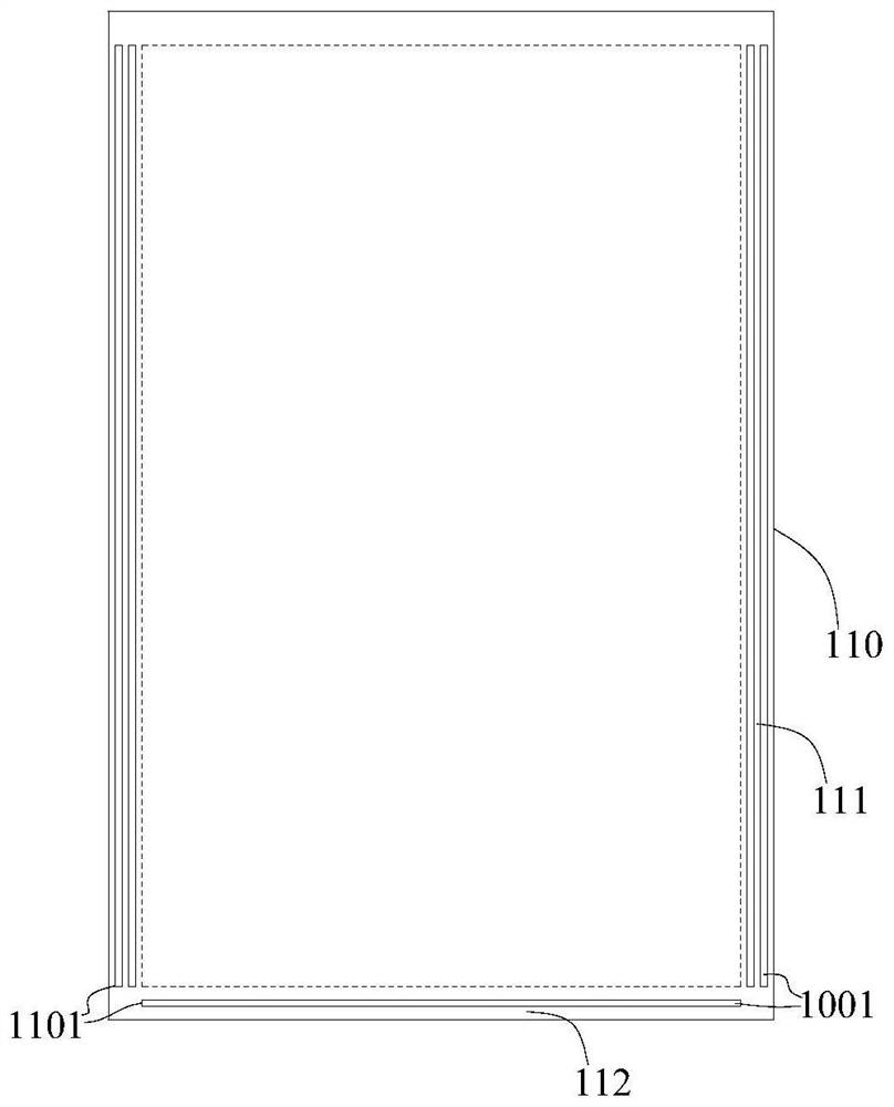
[0062] Figure 4 A schematic diagram of the distribution of the first microstructure on the backplane provided in Embodiment 2 of the present invention, combined with figure 2 with Figure 4 As shown, Embodiment 2 of the present invention provides a display device 10. The structure of the display device 10 is similar to that of the display device 10 provided in Embodiment 1 of the present invention. This embodiment will not repeat the same parts. The difference is that the The distribution modes of the grooves 1001 in the microstructure 1000 on the display panel 100, the backplane 110 and the composite functional layer of the above-mentioned display devices are different.

[0063] Specifically, the microstructure 1000 includes the first microstructure 1101 disposed on the edge of the backplane 110, the second microstructure 1221 disposed on the edge of the composite functional layer, and the The third microstructure 1011 on the edge of the display panel 100 is described abo...

Embodiment 3

[0069] Figure 5 A schematic diagram of the distribution of the first microstructure on the backplane provided in Embodiment 3 of the present invention, combined with figure 2 with Figure 5 As shown, Embodiment 3 of the present invention provides a display device 10. The display device 10 is similar in structure to the display device 10 provided in Embodiment 1 of the present invention. This embodiment will not repeat the same parts. The difference is that the The distribution modes of the grooves 1001 in the microstructure 1000 on the display panel 100, the backplane 110 and the composite functional layer of the above-mentioned display devices are different.

[0070] Specifically, the microstructure 1000 includes the first microstructure 1101 disposed on the edge of the backplane 110, the second microstructure 1221 disposed on the edge of the composite functional layer, and the The third microstructure 1011 on the edge of the display panel 100 is described above. The str...


PUM


Abstract

The invention provides a display device. The display device comprises a display panel; the back plate is positioned on one side of the display panel; the composite function layer is located on the side, away from the display panel, of the back plate; wherein the edge of at least one of the display panel, the back plate and the composite functional layer is provided with a microstructure. The edge of at least one of the display panel, the back plate and the composite functional layer is provided with the microstructure, so that the pinning effect and the adhesion effect among the display panel, the back plate and the composite functional layer can be effectively enhanced; therefore, the phenomenon of stripping among the display panel, the back plate and the composite function layer in the disassembly and repair process of the display device is effectively avoided, the disassembly and repair yield of the display device is improved, and the cost is reduced.

Description

technical field [0001] The present invention relates to the field of display technology, in particular to a display device. Background technique [0002] Organic Light Emitting Diode (OLED) display device has low driving voltage, high luminous efficiency, short response time, high definition and contrast, nearly 180° viewing angle, wide operating temperature range, and can realize flexible display and large-area full-screen display. With many advantages such as color display, it is recognized by the industry as the display device with the most development potential. [0003] In order to ensure the stability and waterproof requirements of the complete machine assembly of the OLED display device, in the display device of the prior art, a high-viscosity middle frame glue is usually used to bond and fix the display panel and the middle frame in the display device. The frame adhesive is strong, and the fixing effect is good, but the side of the display panel close to the middle ...

Claims


Application Information

Patent Timeline
Patent Type & Authority Applications(China)
IPC IPC(8): H01L51/52G09F9/33
CPCG09F9/33H10K50/841
Inventor 占栋
Owner WUHAN CHINA STAR OPTOELECTRONICS SEMICON DISPLAY TECH CO LTD
Why Eureka
Try Eureka