Fast comparator circuit with wide common-mode input voltage

A common-mode input voltage and comparator circuit technology, applied in multiple input and output pulse circuits, electrical components, pulse processing, etc., can solve problems such as limiting the maximum transmission rate of signals, reducing edge rates, and affecting signal transmission quality. Achieve the effect of improving signal quality and increasing speed

Active Publication Date: 2022-03-22
成都芯翼科技有限公司
14 Cites 0 Cited by

AI-Extracted Technical Summary

Problems solved by technology

In order to obtain sufficient voltage gain and small input offset voltage, NMOS differential pairs and PMOS differential pairs need to be designed with large device sizes, but large-sized input devices will introduce non-negligible input capacitance
When performing serial or multipoint link signal transmission, the low-pass fil...

Abstract

The invention discloses a fast comparator circuit with a wide common-mode input voltage. The fast comparator circuit comprises a common-mode level control network, a first comparator, a second comparator, an output stage and a capacitance limiting circuit, the common-mode level control network converts the first differential signal into a second differential signal; the input end of the first comparator is connected with the output end of the common-mode level control network in the same direction; the input end of the second comparator is connected with the output end of the first comparator in the same direction; the input end of the output stage is connected with the output end of the second comparator in the same direction; the capacitance limiting circuit is connected with a first differential signal and is connected with the input end of the second comparator. According to the invention, very small offset voltage VOS and very high-speed dynamic signal transmission are respectively obtained in a manner of cascading two groups of comparators; therefore, mutual restriction between the offset voltage VOS and the signal transmission rate is avoided, the signal transmission rate is improved on the premise that the more accurate offset voltage VOS is guaranteed, and the signal quality is improved.

Application Domain

Multiple input and output pulse circuits

Technology Topic

Comparators circuitsCapacitance +8

Image

  • Fast comparator circuit with wide common-mode input voltage
  • Fast comparator circuit with wide common-mode input voltage
  • Fast comparator circuit with wide common-mode input voltage

Examples

  • Experimental program(1)

Example Embodiment

[0039] Example
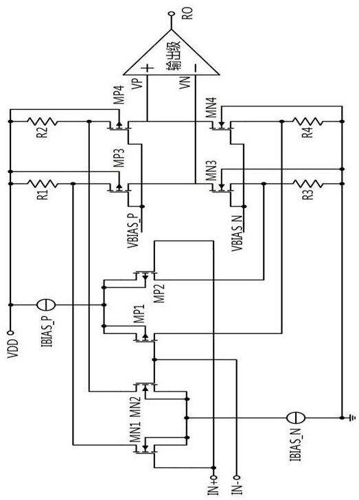
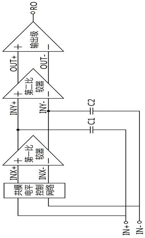
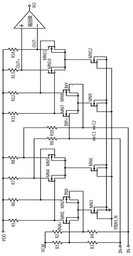
[0040] In order to solve the low-pass filter formed by the input capacitance of the large-sized comparator present in the prior art, it reduces the edge rate, thereby limiting the maximum transmission rate of the signal, and the additional capacitive load brought by the input capacitor causes the receiver input. Extra jitter occurs, which in turn affects the technical problem of signal transmission quality, which provides a fast comparator circuit for a wide co-mode input voltage, which provides small disorders by setting two sets of comparator cascading. Voltage VOS and high-rate dynamic signal transmission. Compare the comparator circuit in the present invention so that the comparator circuit in the present invention is no longer constrained between the offset voltage VOS and the signal transmission rate. Under the premise of ensuring a more accurate offset voltage VOS, the rate of signal transmission is improved, and the signal quality is improved.
[0041] Such as figure 2 and image 3 As shown, this embodiment provides a fast comparator circuit of a wide common mode input voltage, including a common mode level control network, a first comparator, a second comparator, an output stage, and a capacitive limit circuit;
[0042] The input end of the common mode level control network is connected to a first differential signal to convert the first differential signal into a second differential signal having a smaller mode range, and output to the first comparator;
[0043] Specifically, the first differential signal includes a forward terminal IN + and a negative direction IN-, the forward input of the common mode level control network is transmitted into the forward terminal IN + of the first differential signal, said The reverse input of the common mode level control network is connected to the negative end IN of the first differential signal, and the conversion is smaller by transitioning the bus input differential signal through a larger mode range. The second differential signal is processed for subsequent first comparator.
[0044] Preferably, the common mode level control network and the first comparator are connected by a pair of signal line INX + and INX-connections.
[0045] The input end of the first comparator is connected to the output of the common mode level control network for comparing the second differential signal to determine the flip point, and outputs a signal to the second comparator;
[0046] Specifically, the forward input of the first comparator is connected to the forward output of the common mode level control network, the reverse input of the first comparator and the common mode level control network. The reverse output is connected to determine the flip point and output the corresponding result to the second comparator by comparing the relationship between the second differential signal and the voltage threshold. At this point, the first comparator can select a large size of the device to make the first comparator input offset voltage VOS easier to obtain accurate control.
[0047] Preferably, the first comparator and the second comparator are connected by a pair of signal lines iny + and iny-connections.
[0048] The input end of the second comparator is connected to the output of the first comparator for transmitting the output signal of the first comparator to the output stage to control the output level;
[0049] Specifically, the forward input of the second comparator is connected to the forward output of the first comparator, the reverse input of the second comparator and the reverse output of the first comparator. The end connection, by receiving the output signal of the first comparator, and transmitted to the output stage, the output level of the output signal can be controlled.
[0050] Preferably, the second comparator and the output stage are connected by a pair of signal lines OUT + and OUT-.
[0051] The input terminal of the output stage is connected to the output of the second comparator for enlarged the output signal of the second comparator, and outputs CMOS as an output driving stage (Complementary Metal OxideMiconductor, complementary metal) Oxide semiconductor) signal;
[0052] Specifically, the forward input terminal of the output stage is connected to the forward output of the second comparator, and the reverse input of the output stage is connected to the reverse output of the second comparator. The output signal of the second comparator is enlarged and the output CMOS signal is used as the drive signal of the receiver.
[0053] The first end of the capacitor limit circuit is accessed to the first differential signal, and the second end of the capacitive limit circuit is connected to the input end of the second comparator.
[0054] Specifically, the first end of the capacitor limit circuit is respectively connected to the forward terminal IN + and a negative direction IN + of the first differential signal, and the second end of the capacitor restriction circuit is respectively associated with the second comparator, respectively. The forward input and the reverse input connection are used to limit the input capacitance of the first differential signal.
[0055] Based on the above disclosure, the present embodiment obtains a small offset voltage VOS and a very high rate dynamic signal transmission by setting two sets of comparator cascading. Compare the comparator circuit in the present invention so that the comparator circuit in the present invention is no longer constrained between the offset voltage VOS and the signal transmission rate. Under the premise of ensuring a more accurate offset voltage VOS, the rate of signal transmission is improved, and the signal quality is improved.
[0056] In a specific embodiment, the capacitor restriction circuit includes a first capacitor C1 and a second capacitor C2, and both ends of the first capacitor C1 respectively correspond to the forward terminal IN + and the first differential signal, respectively. The forward input of the second comparator is connected, and both ends of the second capacitor C2 are connected to the negative input end of the first differential signal, respectively, and the negative input end of the second comparator.
[0057] In a specific embodiment, the common mode level control network includes a first resistor R1, a second resistance R2, a third resistance R3, and a fourth resistor R4;
[0058] The first end of the first resistor R1 is connected to the first end of the common mode reference voltage Vcm and the second resistor R2, and the second end of the first resistor R1 respectively corresponds to the forward direction of the first comparator, respectively. The first end of the input and the third resistor R3 is connected, and the second end of the third resistor R3 is accessed into the forward terminal IN + of the first differential signal;
[0059] The first end of the second resistor R2 is accessed into the common mode reference voltage Vcm, and the second end of the second resistor R2 is respectively related to the reverse input of the first comparator and the fourth resistance. The first end is connected; the second end of the fourth resistor is accessed into the negative direction IN of the first differential signal.
[0060] In a specific embodiment, the first resistor R1 is equal to the second resistance R2 resistance, and the third resistor R3 is equal to the fourth resistor R4 resistance, and the first comparison is at this time. The ideal disorder voltage VOS = 0V.
[0061] In a specific embodiment, the first comparator includes a first NMOS tube MN1, a second NMOS tube MN2, a third NMOS tube MN3, a fourth NMOS tube MN4, a fifth NMOS tube MN5, a sixth NMOS tube Mn6, fifth resistor R5, sixth resistor R6, seventh resistance R7, eighth resistance R8, ninth resistor R9 and tenth resistance R10;
[0062] The gate of the first NMOS tube MN1 is connected to the second end of the second resistor R2 and the first end of the third resistor R3, and the drain end of the first NMOS tube MN1 and the fifth resistor The first end of the R5 and the gate of the fourth NMOS tube MN4 are connected, and after the source end and the substrate of the first NMOS tube MN1 are connected, the source end and the substrate of the second NMOS tube Mn2, respectively. The drain end of the third NMOS tube MN3 is connected, and the second end of the fifth resistor R5 is grounded;
[0063] The drain end of the second NMOS tube MN2 is connected to the first end of the sixth resistor R6 and the gate of the fifth NMOS tube MN5, and the gate of the second NMOS tube MN2 is respectively The second end of the second resistor R2 is connected to the first end of the fourth resistor R4, and the second end of the sixth resistor R6 is connected to the power supply VDD;
[0064] The gate access bias voltage Vbias_n of the third NMOS tube MN3 is grounded from the source terminal and the substrate of the third NMOS tube Mn3;
[0065] The drain end of the fourth NMOS tube MN4 is connected to the first end of the seventh resistor R7 and the first end of the ninth resistor R9, and the source terminal and the substrate of the fourth NMOS tube MN4 are connected. The second end of the seventh resistor R7 is grounded from the source terminal and the substrate of the fifth NMOS tube MN5 and the sixth NMOS tube MN6, and the second end of the seventh resistor R7 is grounded, and the second end of the ninth resistor R9 is respectively. Connect the forward input of the second comparator and the first end of the first capacitor C1;
[0066] The drain end of the fifth NMOS tube MN5 is connected to the first end of the eighth resistance R8 and the first end of the tenth resistor R10, and the second end of the eighth resistor R8 is grounded, the first The second end of the ten resistor R10 is connected to the reverse input of the second comparator and the first end of the di-capacitor C2;
[0067] The source end and substrate of the sixth NMOS tube MN6 are grounded, and the gate of the sixth NMOS tube MN6 is accessed to the bias voltage Vbias_n.
[0068] In a specific embodiment, the second comparator comprises seventh NMOS tube MN7, an eighth NMOS tube MN8, a ninth NMOS tube MN9, tenth NMOS tube MN10, and the eleventh NMOS tube MN11, and the twelfth NMOS tube MN12, the eleventh resistance R11, the twelfth resistor R12, the thirteenth resistance R13 and the fourteenth resistance R14;
[0069] The gate of the seventh NMOS tube MN7 is connected to the second end of the ninth resistor R9 and the first end of the first capacitor C1, and the drain end of the seventh NMOS tube MN7 is respectively The first end of the eleventh resistor R11 and the gate of the tenth NMOS tube MN 10 are connected, and the source terminal of the seventh NMOS tube MN7 and the substrate are connected to the source and liner of the eighth NMOS tube MN8, respectively. The bottom end and the drain end of the ninth NMOS tube MN9, the second end of the eleventh resistor R11 accesses the power supply VDD;
[0070] The drain end of the eighth NMOS tube MN8 is connected to the first end of the twelfth resistor R12 and the gate of the eleventh NMOS tube MN11, and the gate electrodes of the eighth NMOS tube MN8 respectively The second end of the tenth resistor R10 is connected to the first end of the second capacitor C2, and the second end of the twelfth resistor R12 is connected to the power supply VDD;
[0071] The gate of the ninth NMOS tube MN9 is accessed to the bias voltage VBIAS_N, the source end and substrate of the ninth NMOS tube MN9;
[0072]The drain end of the tenth NMOS tube MN 10 is connected to the first end of the thirteenth resistor R13 and the output stage of the output stage, and the source end and the substrate of the tenth NMOS tube Mn 10 are connected. The second end of the thirteenth resistor R13 is connected to the drain end of the eleventh NMOS tube MN11 and the drain end of the twelfth NMOS tube Mn12, and the second end of the thirteenth resistor R13 is connected to the power supply VDD;
[0073] The drain end of the eleventh NMOS tube MN11 is connected to the first end of the fourteenth resistor R14 and the inverse input of the output stage, and the second end of the fourteenth resistor R14 is connected to the power supply. VDD;
[0074] The source end and substrate of the twelfth NMOS tube MN12 are grounded, and the gate of the source end of the twelfth NMOS tube MN12 is accessed to the bias voltage Vbias_n.
[0075] Among them, the specific working principle of the rapid comparator circuit of the wide common mode input voltage in this embodiment is as follows:
[0076] First, a wide common mode input voltage range and a low offset voltage VOS parameter are implemented by the circuit structure of the co-mode level control network and the first comparator. Specifically, in the common mode level control network circuit, by reasonably setting the ratio between the first resistor R1 and the third resistor R3, and the second resistance R2 and the fourth resistor R4 The ratio between the first comparator can be controlled in the first NMOS tube N1 and the second NMOS tube N2 to achieve accurate control of the offset voltage. . For example, if the first resistor R1 = second resistor R2, and the third resistor R3 = fourth resistor, the ideal disorder voltage VOS = 0V of the first comparator is fine-tuning the first resistor R1 to the fourth resistor R4. Any resistance of any resistor can easily set the offset voltage to the other desired value, and achieve the precise control of the offset voltage. Further, the differential pair of the first NMOS tube N1 and the second NMOS tube N2 can be selected to obtain a more accurate offset voltage parameter value.
[0077] Next, the high-speed transmission of the signal is realized by the circuit structure of the capacitive limit circuit composed of the second comparator and the first capacitor C1 and the second capacitor C2. Specifically, when the high speed signal is transmitted, the input capacitance of the forward terminal IN + of the first differential signal is approximately a series value of the first capacitor C1 and the second comparator input differential device MN7 parasitic capacitance, so it can be lowered. The capacitance value of the capacitor is input to the end; the input capacitor of the first differential signal is approximated to the second capacitor C2 and the second comparator input differential device MN8 parasitic capacitance, so Reduce the capacitance value of the negative direction input capacitor. Therefore, the input capacitance of the first differential signal is effectively reduced.
[0078] It can be seen that a small offset voltage VOS and a high-rate dynamic signal transmission are obtained by setting two sets of comparator cascading. Compare the comparator circuit in the present invention so that the comparator circuit in the present invention is no longer constrained between the offset voltage VOS and the signal transmission rate. Under the premise of ensuring a more accurate offset voltage VOS, the rate of signal transmission is improved, and the signal quality is improved.

PUM

no PUM

Description & Claims & Application Information

We can also present the details of the Description, Claims and Application information to help users get a comprehensive understanding of the technical details of the patent, such as background art, summary of invention, brief description of drawings, description of embodiments, and other original content. On the other hand, users can also determine the specific scope of protection of the technology through the list of claims; as well as understand the changes in the life cycle of the technology with the presentation of the patent timeline. Login to view more.

Similar technology patents

Three dimensional printer and control method thereof

InactiveUS20150183162A1increase speedprevent implementation
Owner:SAMSUNG ELECTRONICS CO LTD

Light source module

InactiveUS20130119884A1cost reductionincrease speed
Owner:HEP TECH

Classification and recommendation of technical efficacy words

  • Improve signal quality
  • increase speed

Antenna steering method and apparatus for an 802.11 station

InactiveUS20050037822A1improves diversityimprove signal quality
Owner:IPR LICENSING INC

Electrode for acquiring physiological signals of a recipient

InactiveUS20100324405A1improve signal qualityraise profile
Owner:KONINKLIJKE PHILIPS ELECTRONICS NV

Modified Xilinx FPGA power-on reset circuit

InactiveCN103218025Aimprove stabilityImprove signal quality
Owner:BEIJING RES INST OF SPATIAL MECHANICAL & ELECTRICAL TECH

Multi-cell cooperative transmission scheme based on interference utilization

ActiveCN109889238AImprove signal qualityReduce the average symbol error rate
Owner:XI AN JIAOTONG UNIV

Intelligent repeater and communication method based on intelligent repeater

PendingCN107623544AAvoid too strong signal interference base station networkImprove signal quality
Owner:KZ BROADBAND TECH
Why Eureka
Try Eureka