Through hole filling manufacturing process of multilayer board

A production process and multi-layer board technology, which is applied in the fields of printed circuit manufacturing, electrical connection formation of printed components, electrical components, etc., can solve the problems affecting product reliability and copper thickness uniformity, unfavorable fine line production, and restricted space utilization, etc. problems, to achieve the effect of facilitating the production of precision circuits, reducing the reliability risk in the hole, and avoiding the grinding process of the resin plug hole

Pending Publication Date: 2022-04-01
JIANGSU PROVISION ELECTRONICS CO LTD
View PDF0 Cites 2 Cited by
  • Summary
  • Abstract
  • Description
  • Claims
  • Application Information

AI Technical Summary

Problems solved by technology

[0002] Most of the existing multi-layer board products are designed with blind holes and POFV. The bottom of the blind hole design must have a pad. With the development of electronic technology and people's requirements for miniaturization and high precision of electronic products, the existence of the pad will affect the product wiring. , which severely restricts the utilization of space; and the combination of mechanical drilling and POFV technology will affect the reliability of the product and the uniformity of copper thickness, which is not conducive to the production of fine lines

Method used


Image

  • Through hole filling manufacturing process of multilayer board
  • Through hole filling manufacturing process of multilayer board
  • Through hole filling manufacturing process of multilayer board

Examples


Embodiment

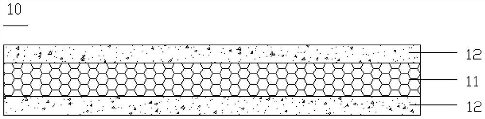
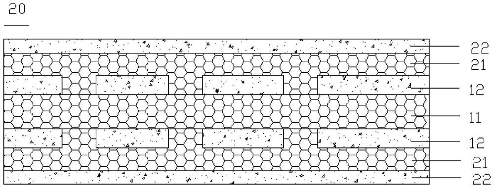
[0052] Example: such as Figure 1-8 Shown, a kind of through-hole filling manufacturing process of multi-layer board comprises the following steps:

[0053] Step 1: cutting and baking: cut a substrate of a certain size, put it in an oven and bake, the substrate 10 is a double-sided copper-clad substrate, and the double-sided copper-clad substrate has an inner insulating layer 11 and two respectively pressing the inner copper foil layer 12 on the front and back sides of the inner insulating layer; figure 1 As shown, the purpose of material cutting is to facilitate subsequent equipment processing; the baking conditions are: the temperature is 122-148°C, and the baking time is 2-4h; the substrate is baked to eliminate the stress of the substrate and prevent the substrate from warping. Improve the dimensional stability of the substrate and reduce the expansion and contraction of the substrate;

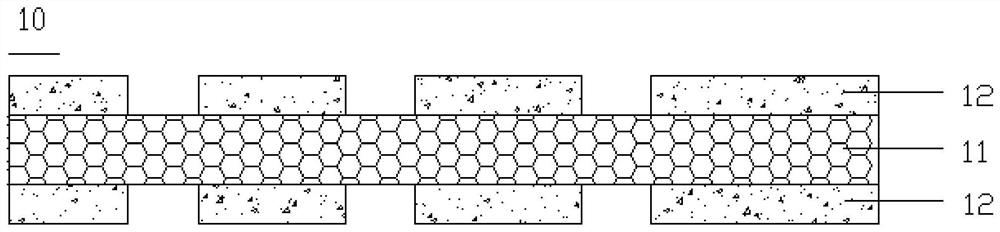
[0054] Step 2: Inner line: eg figure 2 As shown, the two inner copper foil layers ...


PUM


Abstract

The invention relates to a through hole filling manufacturing process of a multi-layer board. The through hole filling manufacturing process comprises the following steps of cutting and baking; in the inner layer circuit, the two inner copper foil layers are subjected to dry film pressing, exposure, development, etching and film stripping treatment, and manufacturing of the inner layer circuit is completed; two-sided pressing: respectively pressing an outer insulating layer and an outer copper foil layer on the two inner copper foil layers to form a four-layer plate; mechanical drilling is conducted, specifically, through holes used for interlayer communication are drilled in the four-layer plate through a drilling machine; pTH: depositing a layer of thin chemical copper on the inner wall of the through hole to realize in-hole conduction; a first outer layer line; filling holes and electroplating; performing grinding; plating copper for the second time; and performing second-time outer-layer circuit manufacturing to complete the manufacturing of the outer-layer circuit. According to the manufacturing process, the reliability of through hole copper plating is improved while the surface copper uniformity of a product is ensured, the pad blocking design of a blind hole is avoided, more design space is provided for customers, and the manufacturing cost is reduced.

Description

technical field [0001] The invention relates to the manufacture of multilayer boards, in particular to a manufacturing process for through hole filling of multilayer boards. Background technique [0002] Most of the existing multi-layer board products are designed with blind holes and POFV. The bottom of the blind hole design must have a pad. With the development of electronic technology and people's requirements for miniaturization and high precision of electronic products, the existence of the pad will affect the product wiring. , which severely restricts the utilization of space; and the combination of mechanical drilling and POFV technology will affect the reliability of the product and the uniformity of copper thickness, which is not conducive to the production of fine lines. Contents of the invention [0003] In order to overcome the above defects, the present invention provides a through-hole filling process for multi-layer boards, which ensures the uniformity of co...

Claims


Application Information

Patent Timeline
IPC IPC(8): H05K3/00H05K3/42
Inventor 马洪伟陆猛
Owner JIANGSU PROVISION ELECTRONICS CO LTD
Why Eureka
Try Eureka