CMOS (complementary metal oxide semiconductor) circuit of memory

A memory and MOS tube technology, applied in static memory, read-only memory, information storage, etc., can solve problems such as reliability risks of high-voltage functional circuits, reduce hot carrier injection effects, improve circuit reliability, and improve endurance The effect of high pressure performance

Pending Publication Date: 2022-04-01
YANGTZE MEMORY TECH CO LTD
View PDF1 Cites 0 Cited by
  • Summary
  • Abstract
  • Description
  • Claims
  • Application Information

AI Technical Summary

Problems solved by technology

[0006] In view of the shortcomings of the prior art described above, the purpose of this application is to provide a memory CMOS circuit for solving the problem of reliability risk in the high-voltage functional circuit in the existing memory CMOS circuit

Method used


Image

  • CMOS (complementary metal oxide semiconductor) circuit of memory
  • CMOS (complementary metal oxide semiconductor) circuit of memory
  • CMOS (complementary metal oxide semiconductor) circuit of memory

Examples


Embodiment 1

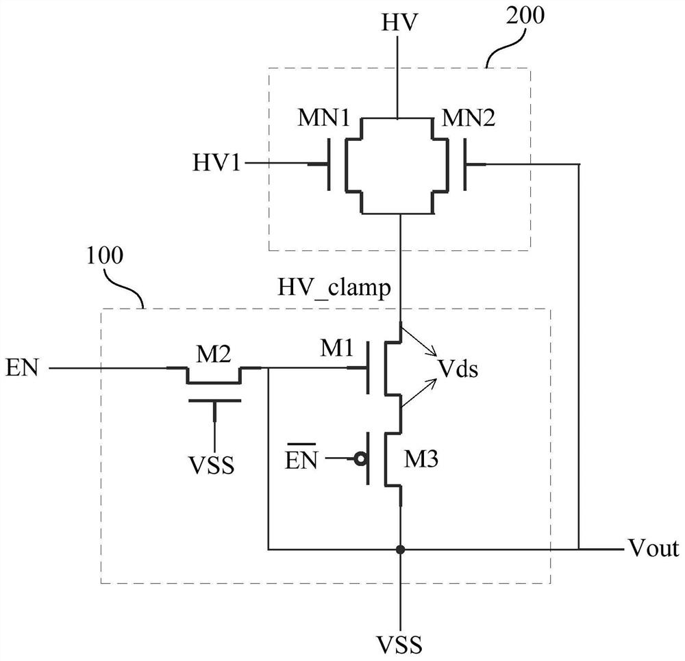
[0029] Such as figure 1 As shown, this embodiment provides a memory CMOS circuit, and the memory CMOS circuit includes:

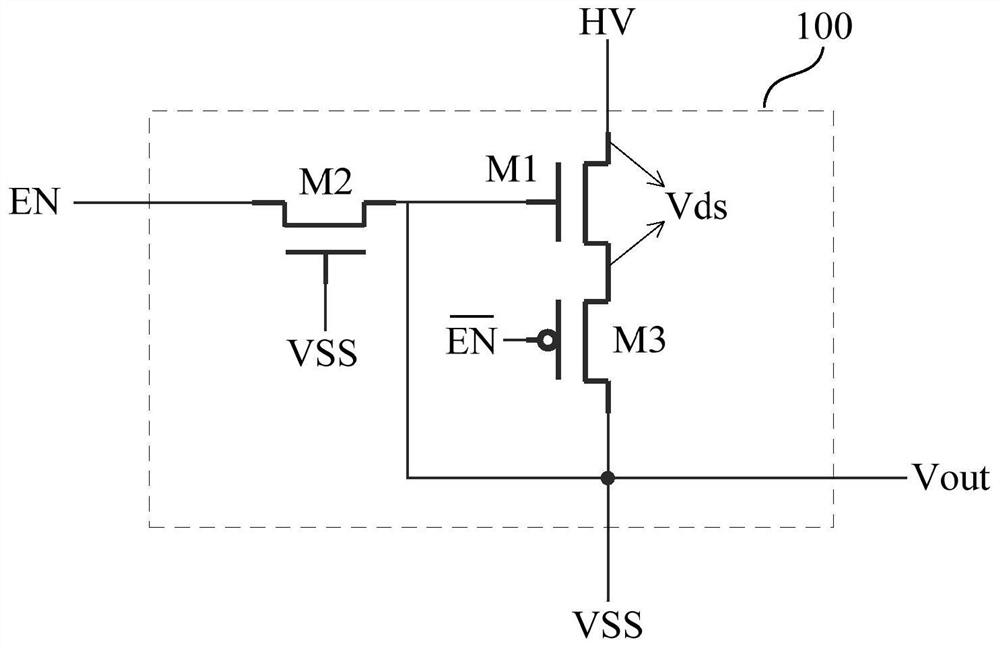
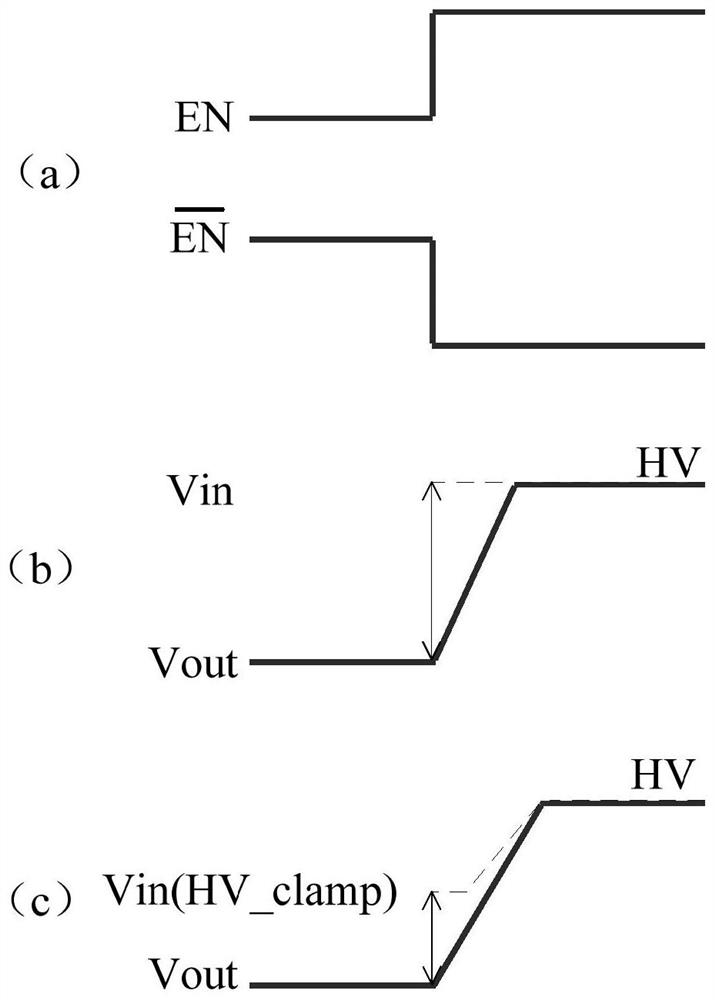
[0030] The high-voltage functional circuit 100 includes at least one MOS transistor, wherein the source terminal or drain terminal of one of the MOS transistors M1 is connected to the input high voltage HV; the high-voltage functional circuit 100 is used to realize that when the enable signal is valid, its output voltage gradually Increase and reach the maximum value HV;

[0031] The auxiliary clamping circuit 200 is arranged between the input high voltage HV and the source terminal or the drain terminal of the MOS transistor M1, and is used for inputting the source terminal or the drain terminal of the MOS transistor M1 during the rising phase of the output voltage. The voltage is clamped so that the clamping voltage HV_clamp is smaller than the input high voltage HV.

[0032] As an example, the high voltage functional circuit 100 includes one of a switc...

Embodiment 2

[0041] Such as Figure 4 As shown, the difference between this embodiment and Embodiment 1 is that the auxiliary clamp circuit 200 in this embodiment further includes: at least one third depletion-type high-voltage NMOS transistor MN3, and the third depletion-type high-voltage NMOS transistor MN3 The first connection end of the first depletion-type high-voltage NMOS transistor MN1 is connected to the first connection end of the first depletion-type high-voltage NMOS transistor MN1, and the second connection end of the third depletion-type high-voltage NMOS transistor MN3 is connected to the first depletion-type high-voltage NMOS transistor MN3. The second connection terminal of the transistor MN1 is connected, and the gate terminal of the third depletion-type high-voltage NMOS transistor MN3 is connected to another preset voltage HV2; wherein, the gate terminal of the third depletion-type high-voltage NMOS transistor MN3 is connected to The preset voltage HV2 is smaller than t...


PUM


Abstract

The invention provides a memory CMOS circuit, and the circuit comprises a high-voltage function circuit which comprises at least one MOS tube, and the source end or drain end of one MOS tube is connected with an input high voltage; when an enable signal is effective, the output voltage is gradually increased and reaches the maximum value; and the auxiliary clamping circuit is arranged between the input high voltage and the source end or the drain end of the MOS tube, and is used for clamping the voltage input to the source end or the drain end of the MOS tube in the rising stage of the output voltage, so that the clamping voltage is smaller than the input high voltage. Through the memory CMOS circuit provided by the invention, the problem that a high-voltage functional circuit in an existing memory CMOS circuit has a reliability risk is solved.

Description

[0001] Cross References to Related Applications [0002] This application is based on a Chinese patent application with application number 202011336570.X and a filing date of November 25, 2020, and claims the priority of this Chinese patent application. The entire content of this Chinese patent application is hereby incorporated by reference into this application. technical field [0003] The application belongs to the field of integrated circuit design, in particular to a memory CMOS circuit. Background technique [0004] In recent years, the development of flash memory (Flash Memory) has been particularly rapid. The main feature of flash memory is that it can keep stored information for a long time without power on, and it has high integration, fast access speed, easy erasing and resetting. It has the advantages of writing and so on, so it has been widely used in many fields such as microcomputer and automatic control. In order to further increase the bit density (Bit Den...

Claims


Application Information

Patent Timeline
Patent Type & Authority Applications(China)
IPC IPC(8): G11C16/04
Inventor 赵利川
Owner YANGTZE MEMORY TECH CO LTD
Why Eureka
Try Eureka