A kind of growth method of superlattice detector material and superlattice infrared detector

A growth method and superlattice technology, applied in polycrystalline material growth, crystal growth, single crystal growth, etc., can solve problems affecting the quality of the interface at the junction of the functional layers of the superlattice detector, the increase of As pressure in the cavity, and the temperature of the cavity Field fluctuations and other problems can be achieved to reduce the growth beam disturbance, improve the utilization rate, and improve the uniformity of components

Active Publication Date: 2022-07-22
WUHAN GAOXIN TECH
View PDF0 Cites 0 Cited by
  • Summary
  • Abstract
  • Description
  • Claims
  • Application Information

AI Technical Summary

Problems solved by technology

During the growth process of existing superlattice detector materials, when growing the barrier layer, it is necessary to raise the temperature of the source furnace for the source material required for the growth of the barrier layer to the growth temperature in advance and wait for a long time. On the one hand, it will cause waste of raw materials; This will lead to the increase of As pressure in the cavity, the fluctuation of the temperature field in the cavity, and the disturbance of the growth beam, which will affect the quality of the interface at the junction of the functional layers of the superlattice detector.

Method used


Image

  • A kind of growth method of superlattice detector material and superlattice infrared detector
  • A kind of growth method of superlattice detector material and superlattice infrared detector

Examples


Embodiment Construction

[0026] The technical solutions in the embodiments of the present invention will be clearly and completely described below with reference to the accompanying drawings in the embodiments of the present invention. Obviously, the described embodiments are only a part of the embodiments of the present invention, but not all of the embodiments. Based on the embodiments of the present invention, all other embodiments obtained by persons of ordinary skill in the art without creative efforts shall fall within the protection scope of the present invention.

[0027] In the description of the present invention, it should be understood that the terms "center", "upper", "lower", "front", "rear", "left", "right", "vertical", "horizontal", The orientation or positional relationship indicated by "top", "bottom", "inner", "outer", etc. is based on the orientation or positional relationship shown in the drawings, and is only for the convenience of describing the present invention and simplifying ...


PUM

PropertyMeasurementUnit
surface roughnessaaaaaaaaaa

Abstract

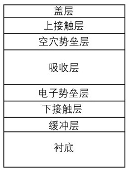
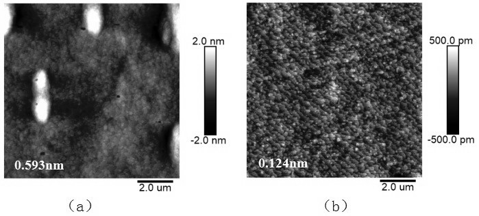
The invention provides a method for growing a superlattice detector material, which includes the following processes: preparing a substrate, and performing high-temperature deoxidation treatment on the substrate in a vacuum growth chamber; growing several supercrystals sequentially from bottom to top on the substrate Lattice detector functional layer, between any two adjacent superlattice detector functional layers, after the growth of the former superlattice detector functional layer is completed, the growth is suspended, and the superlattice surface is treated with V group elements. After the source furnace temperature of the source material required for the growth of the functional layer of the latter superlattice detector is raised to the growth temperature and reaches a stable state, the growth of the functional layer of the latter superlattice detector is completed. In the invention, a growth pause is inserted between the growth of two different superlattice detector functional layers, and at the same time the protection of group V elements is used during the growth pause, which can effectively reduce the fluctuation of the background As pressure and reduce the function of each superlattice detector. The As and Sb elements are mixed between the layers to improve the interface quality at the connection between the functional layers of the superlattice detector.

Description

technical field [0001] The invention belongs to the technical field of semiconductor materials and devices, and particularly relates to a growth method of a superlattice detector material and a superlattice infrared detector. Background technique [0002] Antimonide-based class II superlattice detector materials based on III-V semiconductors are a new type of infrared detector materials, which have the advantages of precise wide-band tunability, high quantum efficiency, good large-area uniformity, high operating temperature, and easy preparation. It has the advantages of low cost and can meet the requirements of the third-generation infrared detector for high detection rate, large area array, multi-band, low power consumption, low cost, etc., so it is the third-generation high-performance infrared focal plane recognized internationally. The preferred material has great potential for development. [0003] In order to effectively suppress SRH dark current, tunneling dark curr...

Claims


Application Information

Patent Timeline
Patent Type & Authority Patents(China)
IPC IPC(8): H01L31/18H01L21/02H01L21/67H01L31/105C30B23/02C30B29/40
CPCY02P70/50
Inventor 黄立吴佳刘永锋王晓碧魏国帅
Owner WUHAN GAOXIN TECH
Why Eureka
Try Eureka