Photoelectric conversion element and imaging device

a technology of photoelectric conversion and imaging device, which is applied in the field of photoelectric conversion element and imaging device, can solve the problems of reducing the aperture ratio and the light collection efficiency, untransmitted light, and poor light utilization efficiency, and achieves high photoelectric conversion efficiency, low dark current, and high responsivity. high

Active Publication Date: 2009-07-30
FUJIFILM CORP
View PDF3 Cites 42 Cited by
  • Summary
  • Abstract
  • Description
  • Claims
  • Application Information

AI Technical Summary

Benefits of technology

[0012]An object of the present invention is to provide an organic photoelectric conversion layer exhibiting high photoelectric conversion effici

Problems solved by technology

In this system, since the color filter transmits only light at a limited wavelength, untransmitted light is not utilized and the light utilization efficiency is bad.
Also, in recent years, amid the advance in fabrication of a multipixel device, the pixel size and in turn, the area of a photodiode part become small and this brings about problems of reduction in the aperture ratio and reduction in the light collection efficiency.
However, the system by the difference in the depth direction of Si is originally disadvantageous in that the color separation is poor, because the absorption range is overlapped among respective portions and the spectroscopic property is bad.
In an attempt to

Method used


Image

  • Photoelectric conversion element and imaging device
  • Photoelectric conversion element and imaging device
  • Photoelectric conversion element and imaging device

Examples


first embodiment

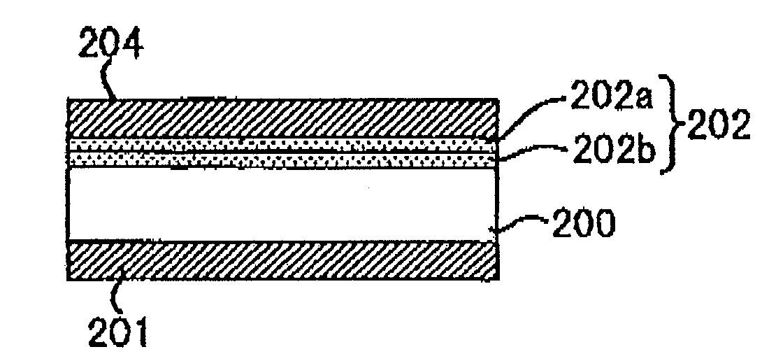
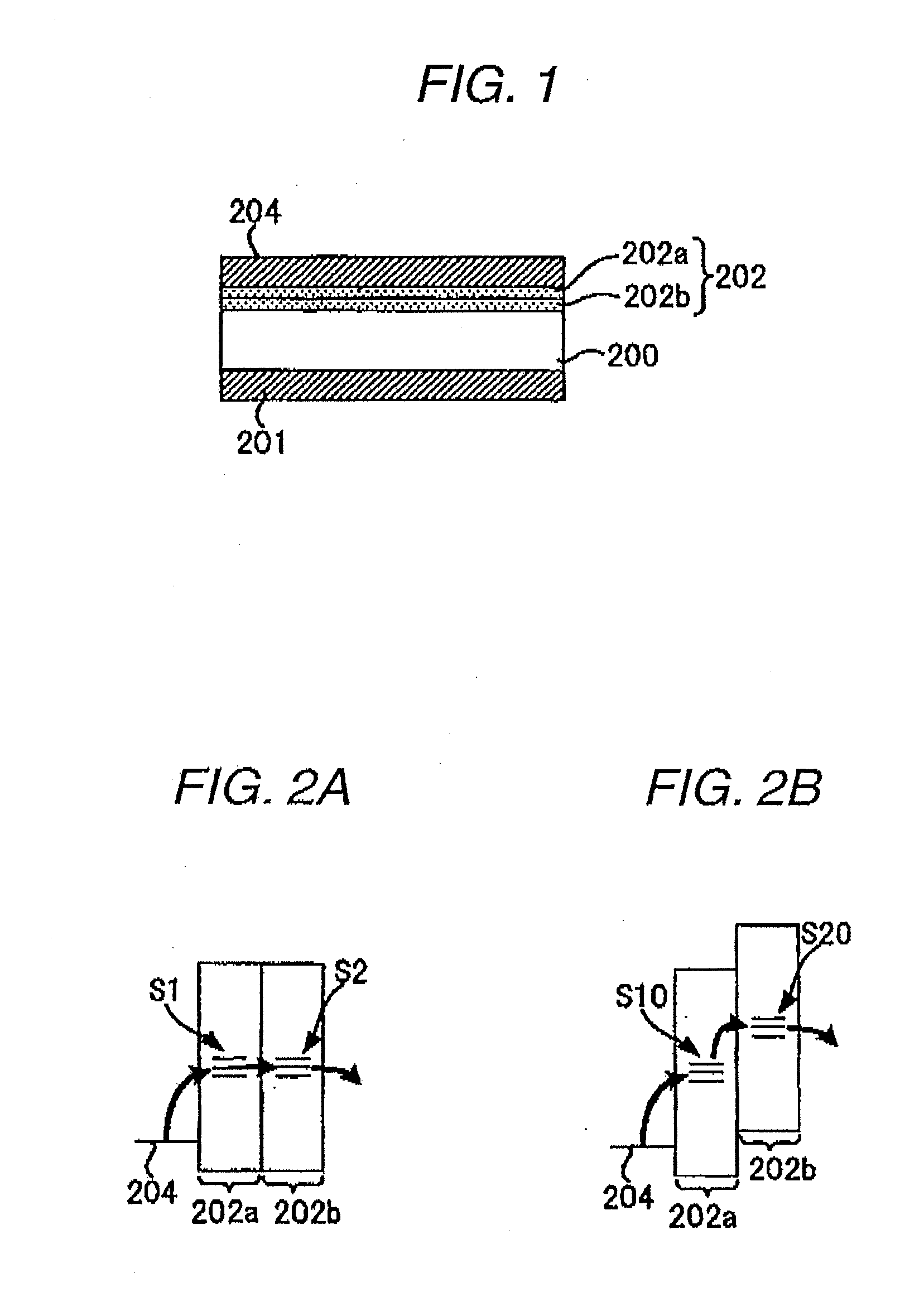
[0292]FIG. 1 is a schematic cross-sectional view showing one example of the construction of the photoelectric conversion element having a charge-blocking layer according to this embodiment.

[0293]In FIG. 1, reference numeral 200 is a photoelectric conversion layer, reference numeral 202 is a charge-blocking layer having a two-layer structure, reference numerals 202a and 202b are layers constituting the charge-blocking layer 202, and reference numerals 201 and 204 are electrodes.

[0294]For example, when the electrode 204 is provided as an electrode on the light incident side, since light needs to be incident into the photoelectric conversion layer 200, the electrode 204 is preferably composed of a material having high transparency. As for the electrode having high transparency, a transparent electrically conductive oxide (TCO) may be used. Similarly, the electrode 201 is preferably composed of a material having high transparency, because as seen in the construction of an imaging device...

second embodiment

[0327]In the second embodiment, a photoelectric conversion element having a charge-blocking layer with a multiple layer structure is specifically described by referring to FIGS. 6 to 11.

[0328]The charge-blocking layer includes “a hole-blocking layer” working as a high barrier to the injection of a hole from the adjacent electrode and exhibiting a high transport ability for an electron that is a photocurrent carrier, and “an electron-blocking layer” working as a high barrier to the injection of an electron from the adjacent electrode and exhibiting a high transport ability for a hole that is a photocurrent carrier. In an organic light-emitting element and the like, as described in JP-A-11-339966 and JP-A-2002-329582, a blocking layer using an organic material is already employed for preventing a carrier from penetrating through a light-emitting layer, but by inserting such an organic blocking layer between an electrode and a photoelectric conversion layer in a photoelectric conversio...

third embodiment

[0363]A construction example of a solid-state imaging device using the photoelectric conversion element having a structure shown in FIG. 11 is described below. In the following, description is made by referring to FIGS. 12 to 16. In each of these Figures, similarly to the above-described embodiments, both the hole-blocking layer and the electron-blocking layer have a multiple layer structure. However, in FIGS. 12 to 16, for drawing convenience, each blocking layer is not illustrated in particular as being divided into a plurality of layers.

[0364]FIG. 12 is a schematic cross-sectional view of one pixel portion of a solid-state imaging device for explaining the third embodiment of the present invention. FIG. 13 is a schematic cross-sectional view of the intermediate layer shown in FIG. 12. In this solid-state imaging device, a large number of pixels, one of which is shown in FIG. 12, are disposed in an array manner in the same plane, and one-pixel data of the image data can be produce...


PUM

PropertyMeasurementUnit
Percent by moleaaaaaaaaaa
Electric fieldaaaaaaaaaa

Abstract

A photoelectric conversion element is provided and includes: an electrically conductive thin layer; an organic photoelectric conversion layer containing a compound having a partial structure represented by the following formula (I) and a fullerene or a fullerene derivative; and a transparent electrically conductive thin layer.
X represents O, S or N—R10, R10 represents a hydrogen atom or a substituent, Rx and Ry represent a hydrogen atom or a substituent, with at least one representing an electron-withdrawing group, Rx and Ry may combine to form a ring, R represents a bond (—), a hydrogen atom or a substituent, with at least one being the bond, nr represents an integer of 1 to 4, R's may be the same or different when nr is 2 or more, and R's at the 2- and 3-positions or R's at the 5- and 6-positions may combine with each other to form a ring.

Description

[0001]This application is based on and claims priority under 35 U.S.C. §119 from Japanese Patent Application No. 2008-015142 filed Jan. 25, 2008, the entire disclosure of which is herein incorporated by reference.BACKGROUND OF THE INVENTION[0002]1. Field of the Invention[0003]The present invention relates to a photoelectric conversion element and provides a photoelectric conversion element with high S / N and high response speed by specifying the materials and structures.[0004]2. Description of Related Art[0005]Conventional visible light sensors in general are a device fabricated by forming a photoelectric conversion site through, for example, formation of PN junction in a semiconductor such as Si. As for the solid-state imaging device, there is widely used a flat light-receiving device where photoelectric conversion sites are two-dimensionally arrayed in a semiconductor to form pixels and a signal generated by photoelectric conversion in each pixel is charge-transferred and read out ...

Claims


Application Information

Patent Timeline
IPC IPC(8): H01L27/00
CPCB82Y10/00H01L27/307H01L51/0046H01L51/0051H01L51/0053H01L51/0061Y10S428/917H01L51/0067H01L51/0072H01L51/4246H01L51/4253H01L2251/308H01L51/0065H10K39/32H10K85/211H10K85/611H10K85/621H10K85/636H10K85/653H10K85/654H10K85/6572H10K30/211H10K30/30H10K2102/103
Inventor MITSUI, TETSURONOMURA, KIMIATSUKITAMURA, TETSU
Owner FUJIFILM CORP
Why Eureka
Try Eureka