
Integrated circuit failure positioning system and method based on continuous laser source

A failure location, integrated circuit technology, used in electronic circuit testing, optical testing flaws/defects, etc., can solve problems such as difficult to locate, resistive failure, transistor gate damage, etc., to achieve reliable positioning results, high positioning accuracy, high The effect of detection efficiency

Inactive Publication Date: 2022-04-12
NAT SPACE SCI CENT CAS
View PDF8 Cites 1 Cited by
  • Summary
  • Abstract
  • Description
  • Claims
  • Application Information

AI Technical Summary

Problems solved by technology

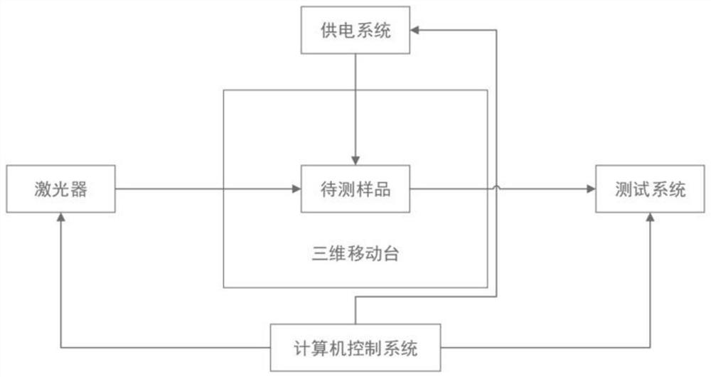
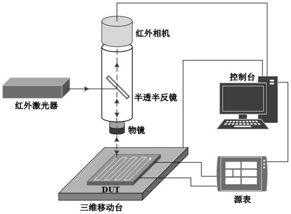
[0004] In order to solve the problems of resistive failure and transistor gate damage that are difficult to locate, the present invention provides the following solution: an integrated circuit failure location system and method based on a continuous laser source, including:

Method used


Image

  • Integrated circuit failure positioning system and method based on continuous laser source
  • Integrated circuit failure positioning system and method based on continuous laser source
  • Integrated circuit failure positioning system and method based on continuous laser source

Examples


Embodiment Construction

[0042] Next, the technical solutions in the embodiments of the present invention will be described in connection with the drawings of the embodiments of the present invention, and it is understood that the described embodiments are merely the embodiments of the present invention, not all of the embodiments. Based on the embodiments of the present invention, all other embodiments obtained by those of ordinary skill in the art are in the range of the present invention without making creative labor premise.

[0043] In order to make the above objects, features, and advantages of the present invention, the present invention will be further described in detail below with reference to the accompanying drawings and specific embodiments.

[0044] An integrated circuit failure positioning method based on continuous laser sources, including:

[0045] The scan data of the circuit sample to be tested by the circuit sample to be tested is obtained based on the 1310nm continuous laser irradiati...


PUM


Abstract

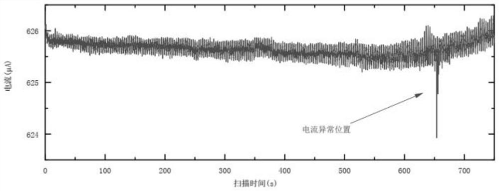
The invention discloses an integrated circuit failure positioning system and method based on a continuous laser source, and the method comprises the steps: irradiating a to-be-detected circuit sample based on an infrared laser, and obtaining the scanning data of the to-be-detected circuit sample; photographing the to-be-detected circuit sample based on an infrared camera to obtain a circuit layout diagram; and comparing the scanning data with the circuit layout diagram to obtain a failure positioning point. According to the method, the failure point positioning problem of the resistive failure of the integrated circuit is solved, and accurate and rapid positioning of the resistive failure of the integrated circuit and transistor grid damage is realized. The test efficiency and the positioning precision of integrated circuit failure positioning are improved, and technical support is provided for research of integrated circuit failure analysis.

Description

Technical field [0001] The present invention belongs to the field of integrated circuit failure, in particular, to an integrated circuit failure positioning system and method based on a continuous laser source. Background technique [0002] Modern integrated circuits have a very broad application. For integrated circuits, it is important to ensure that it is very important for long-term stability. The standard, which is measured, called the reliability of the integrated circuit. The reliability is high, and most of them depends on the manufacturing quality of the integrated circuit. In modern integrated circuit manufacturing techniques, the manufacture of chips requires a series of process, each process, may introduce different defects in chips. The existence of defects does not necessarily lead to direct damage to the chip, and more likely to fail in a certain or several specific units. In the wafer test and package test phase of the chip, the failure of the failure of the fault...

Claims


Application Information

Patent Timeline
Patent Type & Authority Applications(China)
IPC IPC(8): G01N21/95G01R31/28
CPCG01N21/95G01R31/28
Inventor 陈睿韩建伟杨涵陈钱梁亚楠马英起上官士鹏朱翔李悦
Owner NAT SPACE SCI CENT CAS
Learn More