
Balanced photoelectric detector binary array optical fiber coupling structure and manufacturing method

A technology of photodetectors and array optical fibers, applied in the coupling of optical waveguides, optical components, instruments, etc., can solve the problems of large coupling part size, high difficulty in coupling process operation, large chip unit spacing, etc., to improve common mode rejection The effect of reducing the difficulty of the coupling process and reducing the size of the coupling package

Active Publication Date: 2022-04-12
THE 44TH INST OF CHINA ELECTRONICS TECH GROUP CORP
View PDF15 Cites 2 Cited by
  • Summary
  • Abstract
  • Description
  • Claims
  • Application Information

AI Technical Summary

Problems solved by technology

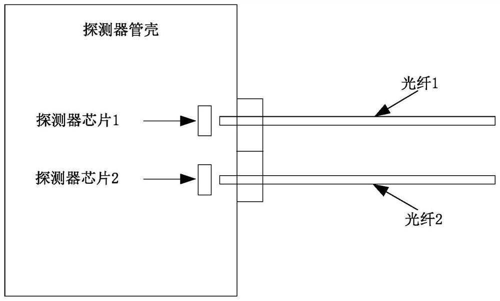
[0004] 1. Independent coupling of two optical fibers makes the coupling process operation difficult;
[0005] 2. The size of the coupling part is large, which is not conducive to the further miniaturization and integration of the balanced photodetection module;
[0006] 3. The distance between the two optical fibers is large, which makes the distance between the chip units in the balanced photoelectric detection module large, which is not conducive to the improvement of the bandwidth performance of the balanced photoelectric detection module;
[0007] 4. The inconsistency of the length of the two optical fibers will degrade the common mode rejection ratio parameter of the balanced photodetection module

Method used


Image

  • Balanced photoelectric detector binary array optical fiber coupling structure and manufacturing method
  • Balanced photoelectric detector binary array optical fiber coupling structure and manufacturing method
  • Balanced photoelectric detector binary array optical fiber coupling structure and manufacturing method

Examples


Embodiment Construction

[0036] The following will clearly and completely describe the technical solutions in the embodiments of the present invention with reference to the drawings in the embodiments of the present invention. Apparently, the described embodiments are only some of the embodiments of the present invention, but not all of them. Based on the embodiments of the present invention, all other embodiments obtained by persons of ordinary skill in the art without making creative efforts belong to the protection scope of the present invention.

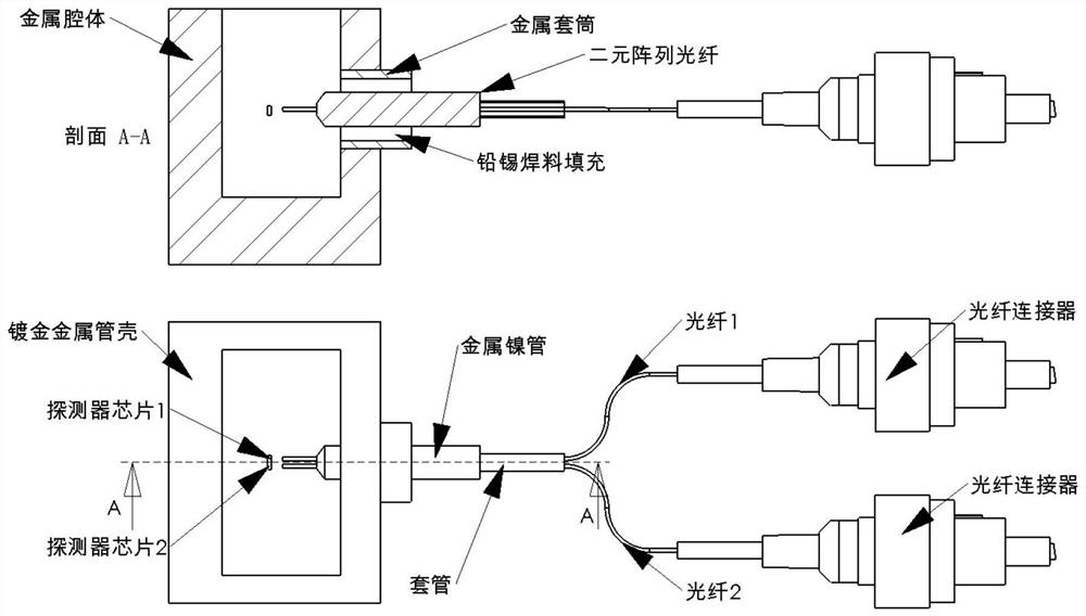
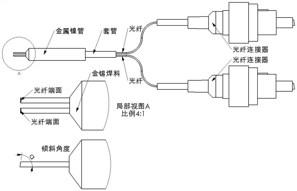
[0037] The invention provides a balanced photodetector binary array optical fiber coupling structure. The binary array optical fiber is welded in a metal shell by using a lead-tin welding process; the metal shell includes a metal sleeve and a metal cavity, and the metal sleeve penetrates embedded in the wall of the metal cavity; the binary array optical fiber includes two optical fibers, metal nickel tube, sleeve and two optical fiber connectors, and the...


PUM

PropertyMeasurementUnit
lengthaaaaaaaaaa
lengthaaaaaaaaaa
diameteraaaaaaaaaa

Abstract

The invention belongs to the technical field of semiconductor packaging, and relates to a binary array optical fiber coupling structure of a balanced photoelectric detector and a manufacturing method, and the coupling structure adopts a lead-tin welding technology to weld a binary array optical fiber in a metal tube shell; the metal tube shell comprises a metal sleeve and a metal cavity, and the metal sleeve is embedded in the wall of the metal cavity in a penetrating mode. The binary array optical fiber comprises two optical fibers, a metal nickel tube, a sleeve and two optical fiber connectors, the two optical fibers are jointly fixed in the metal nickel tube by adopting a gold-tin welding process, one ends of the two optical fibers are exposed out of the metal nickel tube, the other ends of the two optical fibers are respectively connected with the optical fiber connectors, and the sleeve wraps the two optical fibers and is connected with the metal nickel tube; the binary array optical fiber is fixed in the metal sleeve, and the metalized end of the binary array optical fiber is coaxially aligned with the photosensitive surface of the chip in the metal cavity; according to the invention, double-fiber coupling can be realized at one time, and the coupling process difficulty is reduced; the coupling packaging size can be reduced, and miniaturization packaging of the photoelectric detection module can be balanced.

Description

technical field [0001] The invention belongs to the technical field of semiconductor packaging, and relates to a balanced photodetector binary array fiber coupling structure and a manufacturing method. Background technique [0002] With the application of information coherent laser communication technology in optical communication, the balanced photodetector, one of the core components of the receiving end, is required to have the characteristics of high bandwidth, high common-mode rejection ratio and integrated miniaturization. [0003] The existing balanced photodetectors mainly use two independent optical fibers of the same length for coupling respectively, such as figure 1 shown. However, in practical applications, the above coupling structure has the following problems: [0004] 1. Independent coupling of two optical fibers makes the coupling process operation difficult; [0005] 2. The size of the coupling part is large, which is not conducive to the further miniatu...

Claims


Application Information

Patent Timeline
Patent Type & Authority Applications(China)
IPC IPC(8): G02B6/42G02B6/245G02B6/26
CPCY02P70/50
Inventor 周浪崔大健任丽严银林
Owner THE 44TH INST OF CHINA ELECTRONICS TECH GROUP CORP
Learn More