Pedestal grounding detection device and method

A technology of ground detection and base, which is applied in the direction of measuring device casing, short circuit test, ion implantation plating, etc., can solve problems affecting wafer quality, affecting wafer electrical performance, affecting product quality, etc.

Pending Publication Date: 2022-04-15
BEIJING NAURA MICROELECTRONICS EQUIP CO LTD
View PDF0 Cites 1 Cited by
  • Summary
  • Abstract
  • Description
  • Claims
  • Application Information

AI Technical Summary

Problems solved by technology

[0005] In the process of performing the process, if the base 4 is short-circuited with the chamber wall 9 or the inner liner 2, for example, foreign objects appear in the chamber to short-circuit the base 4 with the chamber wall 9 or the inner liner 2, or the base 4 and the inner liner 2 are short-circuited. When the pressure ring 3 is not completely separated from the inner liner 2, it is misjudged that the base 4 has reached the process position and the magnetron sputtering process is started. At this time, the base 4 is short-circuited with the chamber wall 9 and the inner liner 2. The accumulated free electrons will be quickly absorbed by the ground, making the base 4 and the ground equipotential, and the chamber wall 9 is connected to the ground, which is equivalent to the base 4 becoming an anode, causing the base 4 and the target 1 (cathode) ) form a current loop, and the current flows through the wafer 7 placed on the base 4, which will cause the components on the wafer 7 to be broken down by the current, which will seriously affect the electrical performance of the wafer and affect the product quality.
In the prior art, it is difficult to find the short circuit between the base 4 and the chamber wall 9 or the inner liner 2 in time during the execution process, so it is impossible to find out the abnormal grounding of the base in time and stop the execution process in time, which affects the quality of the wafer

Method used


Image

  • Pedestal grounding detection device and method
  • Pedestal grounding detection device and method
  • Pedestal grounding detection device and method

Examples


Embodiment Construction

[0043] The present application will be described in more detail below with reference to the accompanying drawings. Although preferred embodiments of the present application are shown in the drawings, it should be understood that the present application may be embodied in various forms and should not be limited to the embodiments set forth herein. Rather, these embodiments are provided so that this application will be thorough and complete, and will fully convey the scope of this application to those skilled in the art.

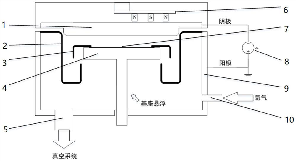
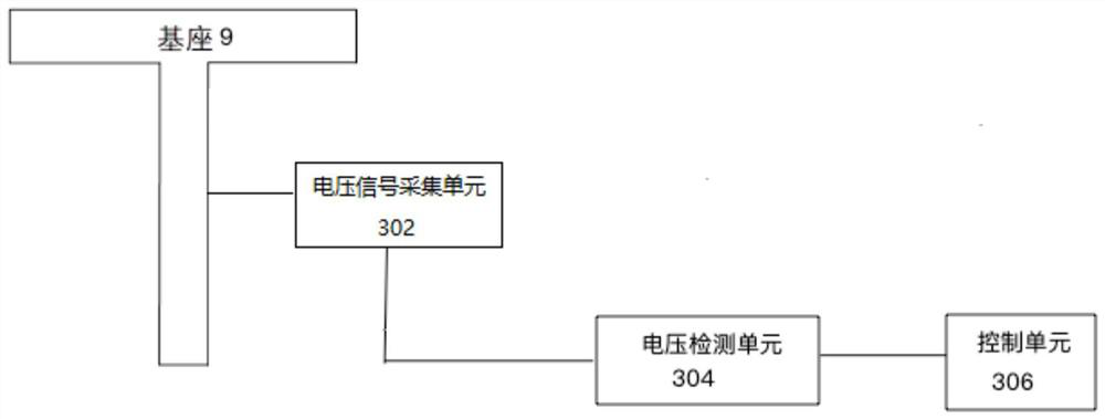
[0044] Please refer to image 3 . image 3 A structural block diagram of a base grounding detection device according to an embodiment of the present application is shown. The device is used in semiconductor equipment, and the base is arranged in a process chamber for semiconductor process in the semiconductor equipment, and the base is used for carrying wafers to be processed. As shown in the figure, the base ground detection device includes a voltage signa...


PUM


Abstract

The invention relates to a pedestal grounding detection apparatus and method. A voltage signal of a base is acquired through a voltage signal acquisition unit, and a voltage detection unit determines whether to take a first signal indicating that the base is grounded as an output signal or not according to the voltage signal and a preset voltage signal; and once the control unit receives the first signal, the control unit immediately indicates the semiconductor equipment to stop executing the process and sends out an alarm signal, so that the grounding condition caused by short circuit between the base and the chamber wall or the lining and the like can be found in time, and the accidents that the electrical performance of the wafer is seriously influenced and the product quality is influenced because the wafer is broken down by current are avoided.

Description

technical field [0001] The present application relates to the field of semiconductor manufacturing, in particular to a base grounding detection device and method. Background technique [0002] The magnetron sputtering process is a technology widely used in the field of semiconductor manufacturing. A typical magnetron sputtering process is figure 1 done inside the high vacuum chamber shown. The main structure of the chamber includes: a chamber wall 9 , a target 1 , a lining 2 , a pressure ring 3 , and a base 4 . These structures mainly constitute the closed environment required for the magnetron sputtering process. Before performing the magnetron sputtering process, the wafer 7 is placed on the base 4, and then the vacuum pump 5 sucks the chamber into a vacuum state. When the chamber reaches a specified vacuum degree, the base 4 will rise and push up the pressure ring 3, so that the pressure ring 3 is separated from the inner liner 2, and the base 4 and the pressure ring 3...

Claims


Application Information

Patent Timeline
Patent Type & Authority Applications(China)
IPC IPC(8): G01R31/52G01R1/04C23C14/35C23C14/50C23C14/54
CPCG01R31/52G01R1/04C23C14/50C23C14/54C23C14/35
Inventor 吴启东
Owner BEIJING NAURA MICROELECTRONICS EQUIP CO LTD
Why Eureka
Try Eureka