Continuous variable-rate satellite communication transponder system based on FPGA (Field Programmable Gate Array)
A transponder system and satellite communication technology, which is applied in the field of satellite communication, can solve the problem of inflexible forwarding rate, achieve high-performance communication forwarding, reduce system resource consumption, and low resource consumption
- Summary
- Abstract
- Description
- Claims
- Application Information
AI Technical Summary
Problems solved by technology
Method used
Image
Examples
Embodiment 1
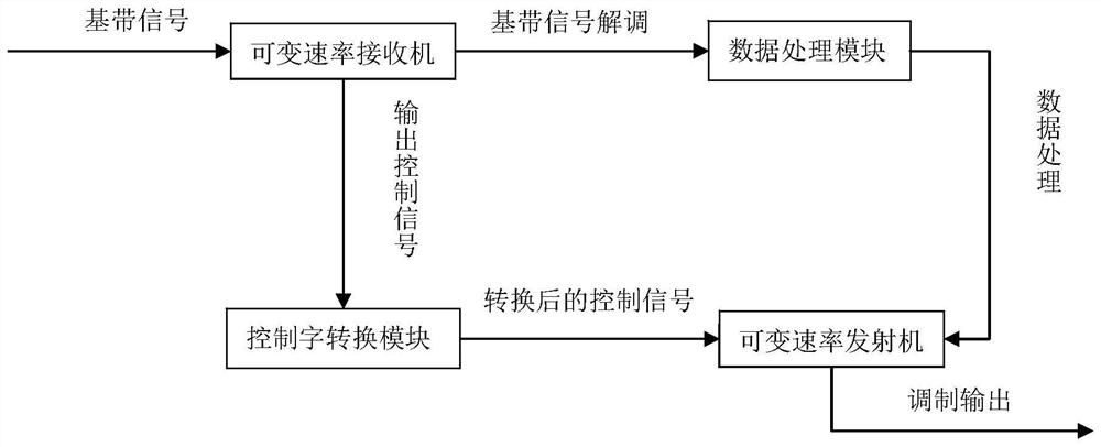
[0049] This embodiment provides a continuously variable rate satellite communication transponder system based on FPGA, combined figure 2 This embodiment can be better understood, the transponder system includes: a variable rate receiver, a data processing module, a control word conversion module and a variable rate transmitter;
[0050] The transponder system receives a continuously variable rate baseband signal and inputs it to the variable rate receiver for demodulation, the demodulated signal is input to the data processing module for data processing, and the processed data is output to the A variable rate transmitter; the variable rate receiver also outputs a control signal to the control word conversion module during demodulation, and the control word conversion module converts the received control signal and outputs it to the variable rate transmitter; The variable rate transmitter performs modulation according to the received control signal and the processed data befor...
Embodiment 2
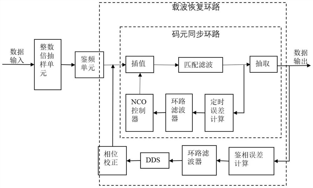
[0053] This embodiment is an example to illustrate the structure of the variable rate receiver in Embodiment 1, combining image 3 This embodiment can be better understood. The variable rate receiver described in this embodiment includes an integer multiple sampling unit, a frequency discrimination unit, a symbol synchronization loop and a carrier recovery loop, and the symbol synchronization loop is embedded in the in the carrier recovery loop;
[0054] The continuously variable rate baseband signal is input to the integer multiple sampling unit for down-sampling, and the down-sampled data is sent to the frequency discrimination unit for coarse frequency synchronization, and the synchronized signal is input to the symbol synchronization unit. The loop performs clock error correction to form a demodulated signal output, and then performs phase error correction through the carrier recovery loop.
[0055] The variable rate receiver described in this embodiment uses an integer m...
Embodiment 3
[0057] This embodiment is to illustrate the specific structure of the integer multiple sampling unit in Embodiment 2. The integer multiple sampling unit structure described in this embodiment is as follows Figure 4 As shown, using FIR filter or CIC+HB filter, the number of sampling stages is selected for the symbol rate of the baseband signal in the way of multi-stage 2 times sampling unit cascading, so that the sampling rate after sampling is 2 to 4 of the symbol rate times.
[0058] The symbol synchronization loop at the back end of the integer multiple sampling unit is processed by a fixed-point number, so when the sampling rate and the multiple of the symbol rate are too different, there are problems of timing error and insufficient interpolation accuracy, and the out-of-band noise will also affect demodulation performance. So the data entering the variable rate receiver needs to be sampled to match the received symbol rate. In this embodiment, in order to adapt to diff...
PUM
 Abstract
Description
Claims
Application Information


