Thin film deposition method

A thin film deposition and thin film technology, applied in ion implantation plating, metal material coating process, coating, etc., can solve the problem of insufficient grain growth energy

Pending Publication Date: 2022-04-19
BEIJING NAURA MICROELECTRONICS EQUIP CO LTD
View PDF6 Cites 1 Cited by
  • Summary
  • Abstract
  • Description
  • Claims
  • Application Information

AI Technical Summary

Problems solved by technology

[0005] The present invention aims to solve at least one of the technical problems existing in the prior art, and proposes a film deposition method, which can solve the problem of insufficient grain growth energy in the central region of the wafer, thereby improving the thickness uniformity of the film, Density and density uniformity, which in turn can improve the corrosion uniformity of the film

Method used


Image

  • Thin film deposition method
  • Thin film deposition method
  • Thin film deposition method

Examples


Embodiment Construction

[0038] In order to enable those skilled in the art to better understand the technical solution of the present invention, the thin film deposition method provided by the present invention will be described in detail below with reference to the accompanying drawings.

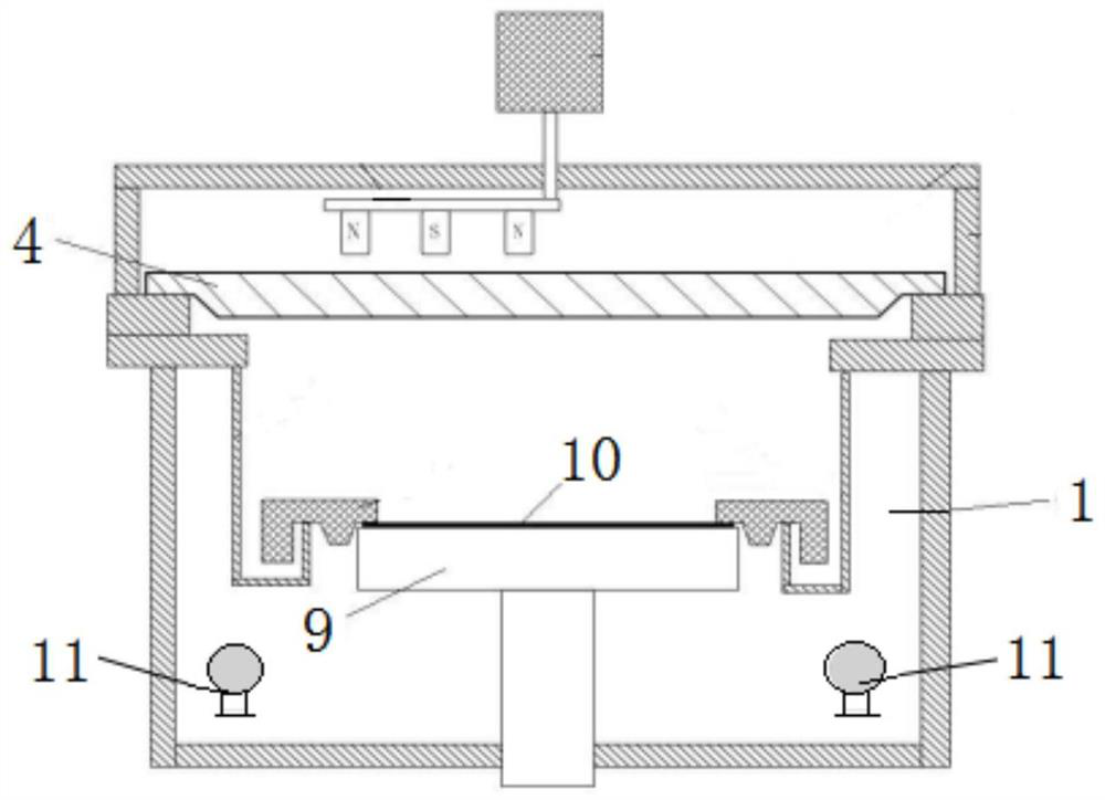
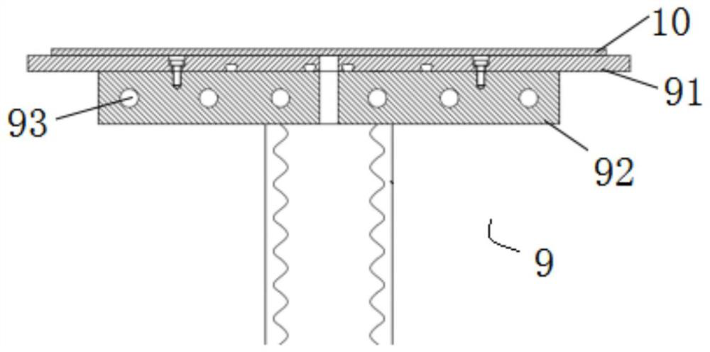
[0039] In the thin film deposition method provided by the embodiment of the present invention, a physical vapor deposition device (Physical Vapor Deposition, PVD) is used to deposit a thin film on a wafer. The physical vapor deposition equipment, for example, adopts figure 1 The shown magnetron sputtering equipment, specifically, the magnetron sputtering equipment includes a reaction chamber 1 , and a liftable base 9 is arranged in the reaction chamber 1 for carrying a wafer 10 . Moreover, a target 4 is arranged on the top of the reaction chamber 1, and the target 4 is electrically connected to a sputtering power supply (not shown in the figure), and the sputtering power supply is used to apply sputtering power to...


PUM

PropertyMeasurementUnit
thicknessaaaaaaaaaa

Abstract

The invention provides a thin film deposition method which comprises the following steps: a ventilation preheating step: introducing sputtering gas into a reaction chamber, starting a heating device in the reaction chamber at the same time, and heating the internal environment of the reaction chamber and the sputtering gas introduced into the reaction chamber; a thin film deposition step: continuously introducing sputtering gas into the reaction chamber, keeping the heating device to be turned on, turning on a sputtering power supply, and loading sputtering power to the target material so as to deposit a thin film on the surface of the wafer arranged on the base; wherein the heating power output by the heating device in the ventilation preheating step is smaller than the heating power output in the thin film deposition step. According to the thin film deposition method provided by the invention, the problem of insufficient grain growth energy in the central area of the wafer can be solved, so that the thickness uniformity, the density and the density uniformity of the thin film can be improved, and the corrosion uniformity of the thin film can be further improved.

Description

technical field [0001] The invention relates to the field of semiconductor manufacturing, in particular to a thin film deposition method. Background technique [0002] Physical vapor deposition (Physical Vapor Deposition, PVD) technology is the most widely used type of thin film manufacturing technology in the semiconductor industry, and generally refers to the thin film preparation process that uses physical methods to prepare thin films. The PVD process in the advanced packaging process is one of the most important processes, which plays a decisive role in the performance of semiconductor devices to a certain extent. [0003] In the flow of a typical advanced packaging process, one of the steps is used to etch the Ti / Cu metal layer not covered by the Cu pillars, but after this step is completed, it often occurs that the Ti / Cu metal layer covered by the Cu pillars will also be etched. Corrosion, leading to the problem of lower product yield. For this reason, it is necessa...

Claims


Application Information

Patent Timeline
Patent Type & Authority Applications(China)
IPC IPC(8): C23C14/35C23C14/16C23C14/06C23C14/54
CPCC23C14/35C23C14/165C23C14/541C23C14/0641
Inventor 张图
Owner BEIJING NAURA MICROELECTRONICS EQUIP CO LTD
Why Eureka
Try Eureka