

Multi-channel signal processing device and method
A signal processing device and multi-channel technology, applied in the field of signal processing, can solve the problems of large size of the whole machine, lack of Internet of Things signal sending and receiving test, and difficulty in meeting outdoor operations, etc., to achieve improved transmission stability, rich external interfaces, The effect of multiple channel requirements
- Summary
- Abstract
- Description
- Claims
- Application Information
AI Technical Summary
Problems solved by technology
Method used
Image

Examples
Embodiment 1
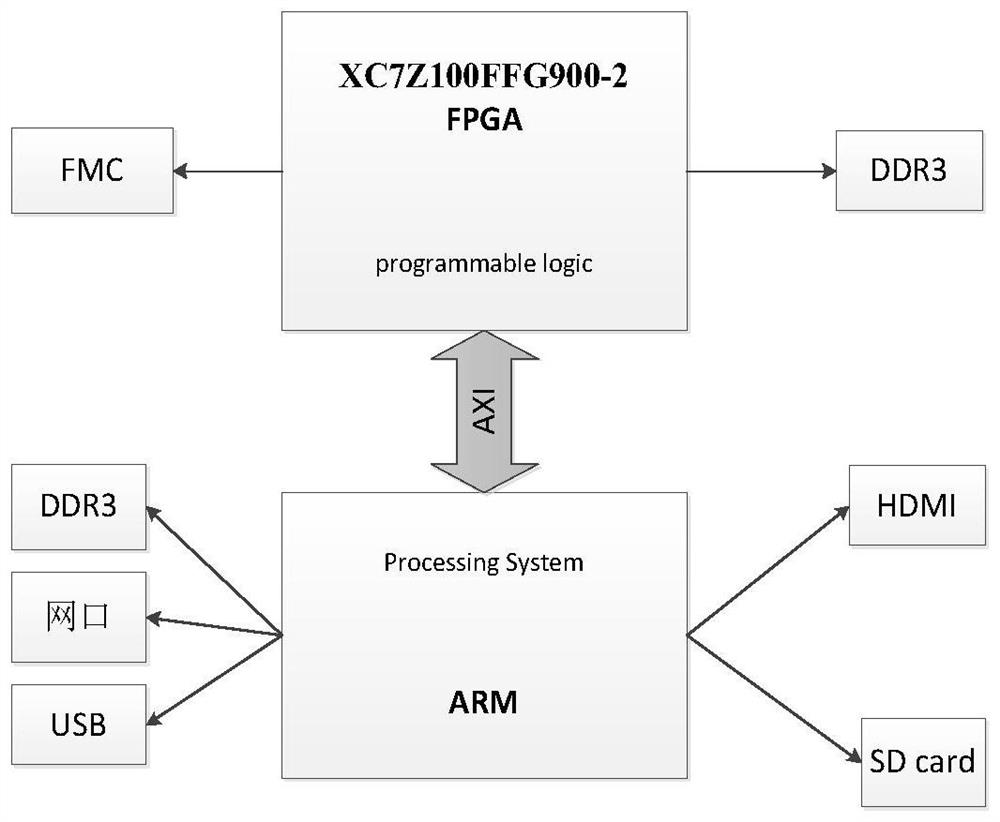
[0038] Such as figure 1 As shown, a multi-channel signal processing device includes a baseband processing module and a radio frequency processing module;
[0039] Baseband processing module, including FPGA, ARM and peripheral interface;
[0040] Peripheral interface, including FMC interface, HDMI port, SD card socket, network port and USB port;
[0041] As the core of data processing, FPGA and ARM are transmitted through the expandable interface AXI bus;
[0042] FPGA configured to control data processing and channels;
[0043] ARM configured for joint processing of data and data interaction with a user manipulation interface;
[0044] FMC interface, configured as a communication channel for FPGA and AD9361 chip;
[0045] The HDMI port is configured to connect to the display screen, which can display and view the operating system in ARM;
[0046] The SD card socket is configured for plugging and unplugging the SD card, where the SD card can realize the programming of the ...
Embodiment 2
[0059] On the basis of the above-mentioned embodiment 1, the present invention also mentions a multi-channel signal processing method, which specifically includes the following steps:
[0060] Step 1: Configure the low-noise amplifier, mixer, low-pass filter, ADC, and DAC in the RF processing module through FPGA to make them work normally;
[0061] Step 2: After the two receiving channels in the AD9361 chip receive the signal, they are sampled, and then the data is transmitted to the FPGA through the FMC interface;
[0062] Step 3: The AD bit width of the AD9361 chip is 12 bits. After zero padding, the data is pieced together into 32 bits and sent to ARM through the AXI bus;
[0063] Step 4: ARM reads the data in real time and transmits it to the network port, and the user control interface performs real-time analysis after receiving the data to realize the signal analysis and demodulation function of the Internet of Things;
[0064] Step 5: The user control interface sends t...
PUM
 Abstract
Description
Claims
Application Information