Multi-time programmable memory and preparation method thereof
A memory and control area technology, applied in semiconductor devices, electrical solid state devices, electrical components, etc., can solve the problems of large device unit area, low coupling efficiency, low efficiency of programming and erasing, and high energy consumption, and achieve increased contact area large, improve programming and erasing efficiency, and reduce device energy consumption
- Summary
- Abstract
- Description
- Claims
- Application Information
AI Technical Summary
Problems solved by technology
Method used
Image

Examples
Embodiment Construction
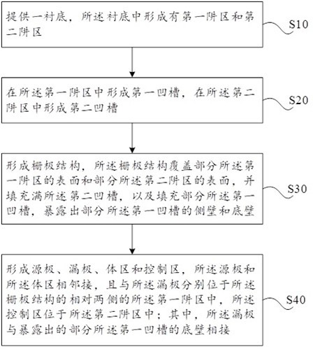
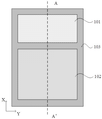
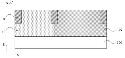
[0041] In order to make the purpose, advantages and features of the present invention clearer, the present invention will be further described in detail below in conjunction with the accompanying drawings and specific embodiments. It should be noted that the drawings are all in very simplified form and not drawn to scale, and are only used to facilitate and clearly assist the purpose of illustrating the embodiments of the present invention. In addition, the structures shown in the drawings are often a part of the actual structure. In particular, each drawing needs to display different emphases, and sometimes uses different scales. It should also be understood that, unless otherwise specified or pointed out, the terms “first”, “second”, “third” and other descriptions in the specification are only used to distinguish each component, element, step, etc. in the specification, rather than It is used to express the logical relationship or sequence relationship between various compo...
PUM
 Abstract
Description
Claims
Application Information
 - R&D
- Intellectual Property
- Life Sciences
- Materials
- Tech Scout
- Unparalleled Data Quality
- Higher Quality Content
- 60% Fewer Hallucinations
Browse by: Latest US Patents, China's latest patents, Technical Efficacy Thesaurus, Application Domain, Technology Topic, Popular Technical Reports.
© 2025 PatSnap. All rights reserved.Legal|Privacy policy|Modern Slavery Act Transparency Statement|Sitemap|About US| Contact US: help@patsnap.com