Variable channel algan/gan HEMT structure and preparation method

A channel and variable technology, applied in semiconductor/solid-state device manufacturing, semiconductor devices, electrical components, etc., can solve problems such as inability to obtain uniform electric field distribution, avoid premature breakdown and failure, and improve withstand voltage performance Effect

Active Publication Date: 2022-07-22
NANJING UNIV OF POSTS & TELECOMM +1
View PDF0 Cites 0 Cited by
  • Summary
  • Abstract
  • Description
  • Claims
  • Application Information

AI Technical Summary

Problems solved by technology

However, the field plate can only achieve the transfer of the peak value of the electric field and cannot obtain a uniform electric field distribution.

Method used


Image

  • Variable channel algan/gan HEMT structure and preparation method
  • Variable channel algan/gan HEMT structure and preparation method
  • Variable channel algan/gan HEMT structure and preparation method

Examples


Embodiment Construction

[0049] The present invention will be described in further detail below with reference to the accompanying drawings and specific preferred embodiments.

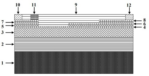
[0050] like figure 1 As shown, a variable channel AlGaN / GaN HEMT structure includes a substrate layer 1, a buffer layer 2, n Set of GaN / AlGaN heterojunction stack, passivation layer 9 , source electrode 10 , gate electrode 11 and drain electrode 12 .

[0051] The material of the above-mentioned substrate layer is preferably silicon, sapphire, gallium nitride or silicon carbide.

[0052] The above buffer layer is epitaxially grown on the top of the substrate layer, preferably a GaN material with a thickness of 2-6 microns.

[0053] n The group GaN / AlGaN heterojunction stacks are epitaxially grown on top of the buffer layer from bottom to top, and from bottom to top are the first group of GaN / AlGaN heterojunction stacks, the second group of GaN / AlGaN heterojunction stacks, ..., the first n Group GaN / AlGaN heterojunction sta...


PUM

PropertyMeasurementUnit
thicknessaaaaaaaaaa
thicknessaaaaaaaaaa
thicknessaaaaaaaaaa

Abstract

The invention discloses a variable channel AlGaN / GaN HEMT structure and a preparation method. A buffer layer is grown on a substrate layer, and a multi-channel layer is regrown on the buffer layer, that is, two or more layers of AlGaN / GaN heterolayers are formed. Then, the multi-channel layer is selectively etched to form a stepped multi-channel layer; then a dielectric passivation layer is deposited on the surface of the device, and chemical and physical polishing is performed to form a stepped passivation layer and top passivation Finally, the metal electrode of the device is prepared by a micro-nano fabrication process to obtain a variable multi-channel AlGaN / GaN HEMT structure.

Description

technical field [0001] The invention relates to a high-voltage power semiconductor, in particular to a variable channel AlGaN / GaN HEMT structure and a preparation method. Background technique [0002] The third-generation semiconductor material GaN is due to its wide band gap (3.39 eV), high electron saturation drift rate (3×10 7 cm / s) and high critical breakdown electric field (3 MV / cm) and other excellent material properties, it has become a popular material for the development of new RF power semiconductor devices. Moreover, thanks to the polarization effect of AlGaN / GaN heterojunction materials, it is possible to obtain high concentration (>1x10 13 cm -2 ), high electron mobility (>1500cm 2 / Vs) two-dimensional electron gas (2DEG). AlGaN / GaN HEMTs have the advantages of large current gain, high cut-off frequency, strong driving capability, low phase noise, and high power density, and have important application prospects in commercial and military fields such a...

Claims


Application Information

Patent Timeline
Patent Type & Authority Patents(China)
IPC IPC(8): H01L29/10H01L29/778H01L21/335
CPCH01L29/1029H01L29/7787H01L29/66462
Inventor 郭宇锋刘建华姚佳飞张珺李曼张茂林
Owner NANJING UNIV OF POSTS & TELECOMM
Why Eureka
Try Eureka