Supercharge Your Innovation With Domain-Expert AI Agents!

Seed crystal layer impurity removal method for DRAM (Dynamic Random Access Memory) evaporation process

A technology of seed crystal layer and impurities, applied in vacuum evaporation plating, metal material coating process, coating and other directions, can solve the problems of poor evaporation effect and ineffective removal, and achieve good evaporation effect.

Inactive Publication Date: 2022-06-24
成都高真科技有限公司
View PDF10 Cites 0 Cited by
  • Summary
  • Abstract
  • Description
  • Claims
  • Application Information

AI Technical Summary

Problems solved by technology

[0005] In order to overcome the deficiencies of the prior art, the present invention provides a method for removing impurities in the seed layer used in the DRAM evaporation process, which solves the problem in the prior art that impurities such as carbon and nitrogen generated during the seeding process cannot be effectively removed, resulting in Problems such as poor evaporation effect

Method used


Image

  • Seed crystal layer impurity removal method for DRAM (Dynamic Random Access Memory) evaporation process
  • Seed crystal layer impurity removal method for DRAM (Dynamic Random Access Memory) evaporation process

Examples


Embodiment 1

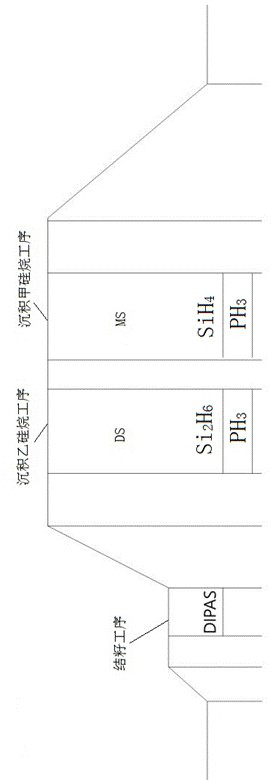
[0023] like figure 1 , figure 2 As shown, a method for removing impurities in a seed crystal layer used in a DRAM evaporation process, after the seed crystal layer is evaporated, the H 2 Annealing process and / or H 2 Remote plasma treatment process.

[0024] This facilitates the effective removal of impurities such as carbon and nitrogen generated during the seed setting process, resulting in a better evaporation effect.

[0025] As a preferred technical solution, it includes a seed setting process, a process of depositing disilane, and a process of depositing monosilane, which are arranged in chronological order. 2 Annealing process and / or H 2 The remote plasma treatment process is provided between the seeding process and the deposition of disilane.

[0026] This facilitates the timely removal of carbon, nitrogen and other impurities generated during the seed setting process after seed setting.

[0027] As a preferred technical solution, H 2 Annealing process and / or H ...

Embodiment 2

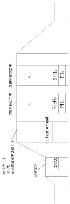
[0044] like figure 1 , figure 2 As shown, as a further optimization of Embodiment 1, this embodiment includes all the technical features of Embodiment 1. In addition, this embodiment also includes the following technical features:

[0045] In order to form a seed layer for evaporating a thin silicon film, it will contain chemicals deposited by DIPAS and SAM24, and contain impurities such as carbon and nitrogen. In order to remove impurities, after evaporating the seed layer, carbon and nitrogen impurities are introduced into H 2 Annealing process or H 2 Remote plasma treatment process removal.

[0046] When vapor deposition is performed during the reaction, H 2 Annealing, the carbon and nitrogen generated after DIPAS are forcibly removed, and the form of contact is filled in the subsequent deposition of DS and MS.

[0047] Preferably, H 2 Annealing after deposition of disilane and removal of SiH 4 can also be done later.

[0048] Preferably, impurities formed between th...


PUM


Abstract

The invention relates to the technical field of semiconductor manufacturing, and discloses a method for removing impurities on a seed crystal layer in a DRAM (Dynamic Random Access Memory) evaporation process, which is characterized in that an H2 annealing process and / or an H2 remote plasma treatment process are / is carried out after evaporation of the seed crystal layer. The problem that in the prior art, carbon, nitrogen and other impurities generated in the seed setting process cannot be effectively removed, so that the evaporation effect is poor is solved.

Description

technical field [0001] The invention relates to the technical field of semiconductor manufacturing, in particular to a method for removing impurities in a seed crystal layer used in a DRAM evaporation process. Background technique [0002] In DRAM, the importance of contact polysilicon (Contact Poly) gap fill (Gap fill) is very high. Especially for seamless (seam free), there have been many improvements in process conditions. One way in the prior art is to generate a seeding layer at the initial stage, and then perform Depo (Deposition, evaporation or deposition) to generate Di-silane (disilane) and Mono-silane (monosilane). In this case, a large amount of DIPAS (Di-isopropylaminosilane, diisopropylamine silane) is used as a seeding chemical, which contains impurities such as carbon and nitrogen. When this impurity is contained in a large amount, subsequent deposition after seeding will be problematic, and evaporation will be difficult. [0003] In DRAM manufacturing, the...

Claims


Application Information

Patent Timeline
IPC IPC(8): C23C14/24C23C14/58H01L21/768
CPCC23C14/24C23C14/5806C23C14/5826H01L21/76883
Inventor 李相遇徐祯秀安重镒
Owner 成都高真科技有限公司
Features
  • R&D
  • Intellectual Property
  • Life Sciences
  • Materials
  • Tech Scout
  • Unparalleled Data Quality
  • Higher Quality Content
  • 60% Fewer Hallucinations
Learn More