Display panel and display device

A display panel and display area technology, applied to static indicators, instruments, semiconductor devices, etc., can solve problems such as display noise, touch recognition failure, and increase in display noise, so as to eliminate influence, ensure normal operation, and eliminate display noise Effect

Pending Publication Date: 2022-06-24
BOE TECH GRP CO LTD
View PDF0 Cites 0 Cited by
  • Summary
  • Abstract
  • Description
  • Claims
  • Application Information

AI Technical Summary

Problems solved by technology

The jump of the data signal transmitted on the data signal line will be coupled to the cathode, causing display noise
[0003] Also, as the size of the display panel increases, display noise also increases
In a display panel with a touch function, especially a display panel with a flexible multi-layer integrated integrated touch technology (Flexible Multi Layer On Cell; FMLOC), since the distance between the touch electrode and the cathode is very close, the touch The load of the second parasitic capacitance formed between the control electrode and the cathode is relatively large, and the display noise will be coupled to the touch electrode through the second parasitic capacitance. In some screens where noise is displayed, the intensity of the display noise is close to the strength of the finger touch signal Or the signal strength of the active pen, causing the touch recognition to fail

Method used


Image

  • Display panel and display device
  • Display panel and display device
  • Display panel and display device

Examples


example 1

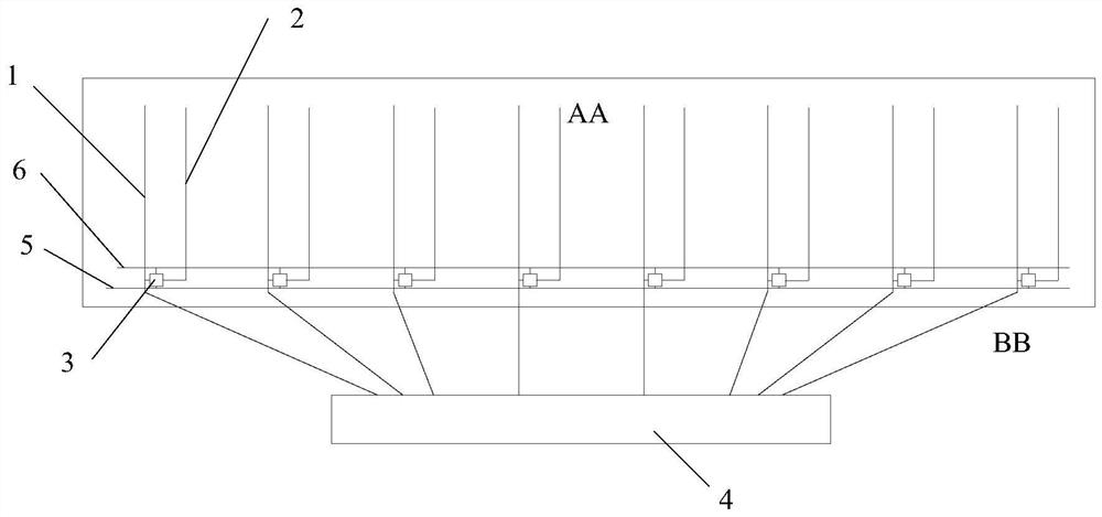
[0074] at least see figure 1 , figure 2 and Figure 4 As shown, the display panel includes a substrate, a pixel structure and a driving circuit; the driving circuit is arranged on the substrate, and the pixel structure is arranged on the driving circuit. According to the actual situation, other layered structures may also be arranged between the substrate, the pixel structure and the driving circuit.

[0075] The display panel includes a display area AA and a non-display area BB surrounding the display area AA. The pixel structure is arranged in the display area AA. The pixel structure includes an anode, a cathode 8, and a luminescent material disposed between the anode and the cathode 8; the cathode 8 is a planar electrode.

[0076] The driving circuit includes a data signal line 1 and a dummy data signal line 2. Each column of pixels corresponds to a data signal line 1 and a dummy data signal line 2. Both the data signal line 1 and the dummy data signal line 2 overlap w...

example 2

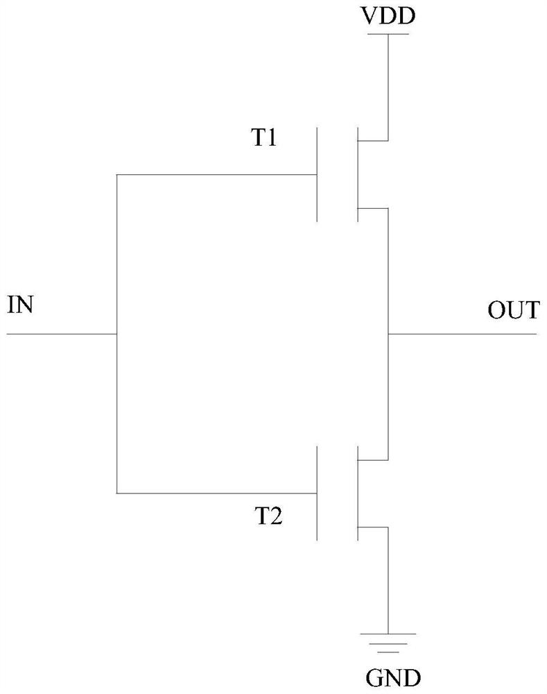
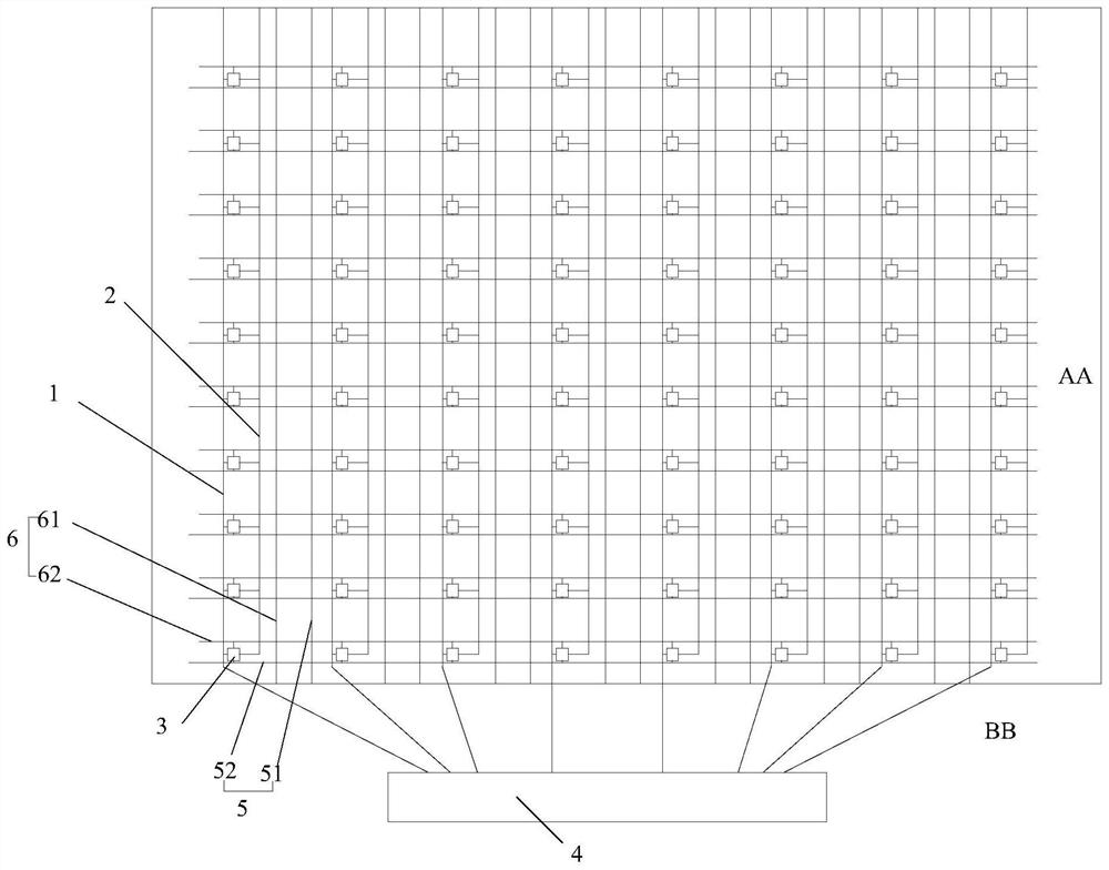
[0082] like image 3 As shown in the figure, the main difference between this example and the above example 1 is that an inverter 3 is provided corresponding to each pixel position, and a first voltage circuit that provides a first voltage for each inverter 3 is set in the display area AA. The line 6 and the second voltage line 5 for supplying the second voltage, the first voltage line 6 and the second voltage line 5 are arranged in a staggered position, wherein the first voltage is the VDD voltage, and the second voltage is the ground voltage.

[0083] The first voltage wiring 6 includes first voltage sub-lines 61 arranged side by side along the first direction and second voltage sub-lines 62 arranged side by side along the second direction; the second voltage wiring 5 includes The third voltage sub-wires 51 arranged side by side in one direction and the fourth voltage sub-wires 52 arranged side by side in the second direction; in the first direction, the first voltage sub-wi...


PUM


Abstract

The invention discloses a display panel and a display device, and the display panel comprises a substrate, a pixel structure and a drive circuit. The pixel structure comprises a cathode; the driving circuit comprises a data signal line and a virtual data signal line, and the data signal line and the virtual data signal line are located on the side, close to the substrate, of the cathode and are both overlapped with the cathode; the phase of a signal on the data signal line is opposite to that of a signal on the virtual data signal line; the display panel further comprises a touch electrode, and the touch electrode is located on the side, away from the substrate, of the cathode and at least partially overlaps with the cathode. According to the scheme, the display noise generated by the signal jump is reduced and even eliminated. Therefore, the influence of the display noise on the touch identification is reduced and even eliminated, and the normal operation of the touch identification is ensured.

Description

technical field [0001] The present invention generally relates to the field of display technology, and in particular, to a display panel and a display device. Background technique [0002] Generally, the cathode of an organic electroluminescence (Organic Light Emitting Diode; OLED) display panel is generally a surface electrode, and the data signal line overlaps with the cathode to form a certain first parasitic capacitance. The transition of the data signal transmitted on the data signal line will be coupled to the cathode, resulting in display noise. [0003] In addition, as the size of the display panel increases, the display noise also increases. In a display panel with touch function, especially a display panel with flexible multi-layer integrated touch technology (Flexible Multi Layer On Cell; FMLOC), due to the close distance between the touch electrode and the cathode, the touch The load of the second parasitic capacitance formed between the control electrode and t...

Claims


Application Information

Patent Timeline
Patent Type & Authority Applications(China)
IPC IPC(8): H01L27/32H01L27/12G09G3/3225G06F3/041
CPCH01L27/1214G09G3/3225G06F3/0412G06F3/0416H10K59/131
Inventor 薄赜文殷新社
Owner BOE TECH GRP CO LTD
Why Eureka
Try Eureka