Flat plate transformer and coupling type self-powered circuit formed by flat plate transformer
A flat-panel transformer, coupled technology, applied in the field of electronics, can solve the problems of large volume and high production cost, and achieve the effects of being less prone to high voltage breakdown, reducing volume and reducing cost
- Summary
- Abstract
- Description
- Claims
- Application Information
AI Technical Summary
Problems solved by technology
Method used
Image
Examples
Embodiment 1
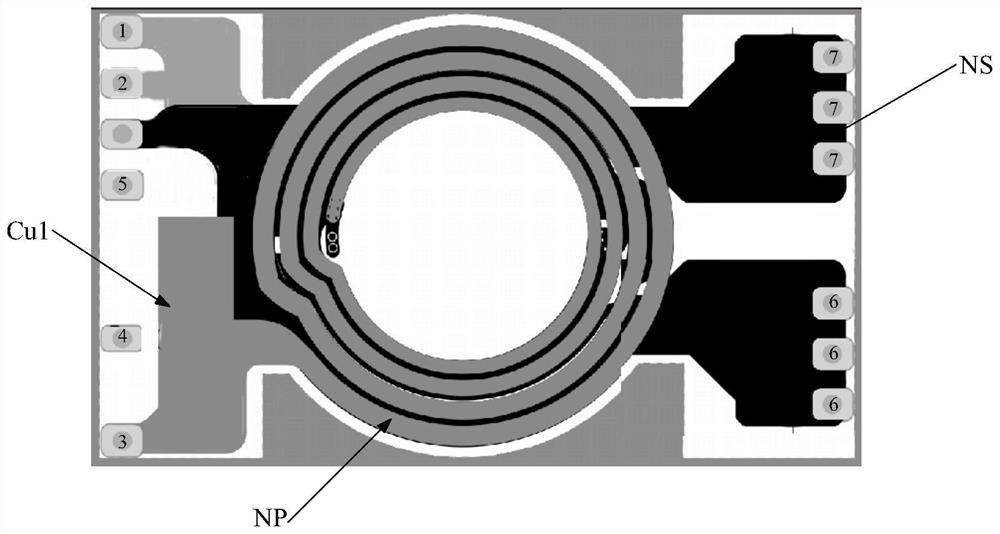
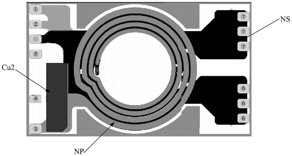
[0020] like figure 1 and figure 2 As shown, the purpose of the present invention is achieved through the following technical solutions: a flat-panel transformer, comprising a primary energy storage winding layer NP and an output winding layer NS. Specifically, the flat-panel transformer in this embodiment cancels the power supply winding layer, which greatly reduces the volume and production cost of the flat-panel transformer. A copper sheet Cu1 is arranged on the lead wire, and the area of the copper sheet Cu1 is larger than the area of the OC lead wire of pin 3 of the primary energy storage winding layer NP. At the same time, the upper and lower layers of the primary energy storage winding layer NP are respectively laid with copper skin Cu2 that matches the copper sheet Cu1, and the copper sheet Cu1 and the copper skin Cu2 are coupled to form a coupling capacitor C1. supply electrode. The copper sheet Cu1 is coupled with the multi-layer and copper skin Cu2 to form th...
Embodiment 2
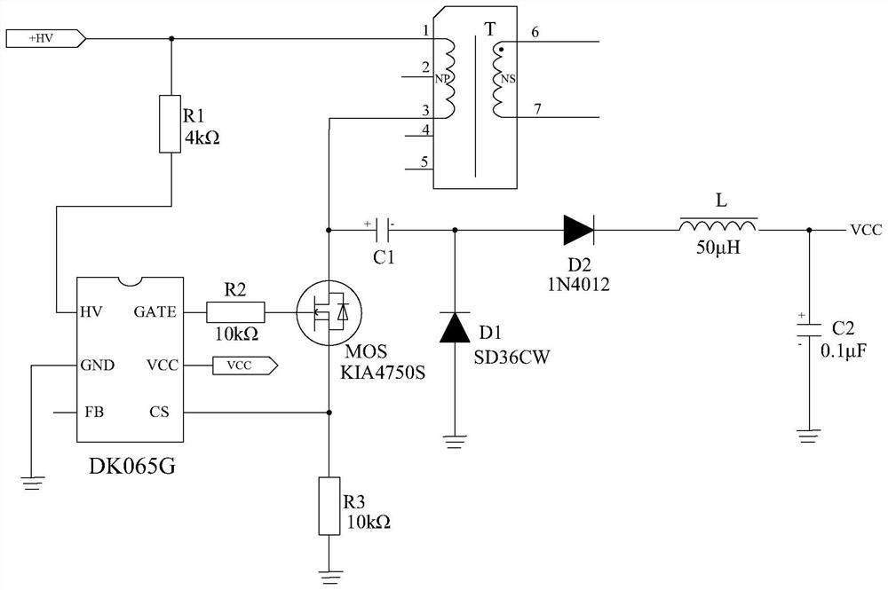
[0023] The coupled self-powered circuit formed by the flat-panel transformer in Embodiment 1 includes a flat-panel transformer, a PWM chip, a field effect transistor MOS, and a charging circuit. like image 3 Specifically, the PWM chip in this embodiment is preferably implemented by the quasi-resonant flyback control AC-DC power switch chip of DK065G, and the field effect transistor MOS is preferentially used as a switching transistor of type KIA4750S, which can be used in actual use. Adjust the model of PWM chip and field effect transistor MOS as needed.
[0024] The gate of the field effect transistor MOS is connected to the GATE pin of the PWM chip through a resistor R2 with a resistance value of 10kΩ. The HV pin of the PWM chip is connected to pin 1 of the primary energy storage winding layer NP through a resistor R1 with a resistance value of 4kΩ. The drain of the field effect transistor MOS is respectively connected with pin 3 of the primary energy storage winding laye...
PUM
 Abstract
Description
Claims
Application Information
 - R&D Engineer
- R&D Manager
- IP Professional
- Industry Leading Data Capabilities
- Powerful AI technology
- Patent DNA Extraction
Browse by: Latest US Patents, China's latest patents, Technical Efficacy Thesaurus, Application Domain, Technology Topic, Popular Technical Reports.
© 2024 PatSnap. All rights reserved.Legal|Privacy policy|Modern Slavery Act Transparency Statement|Sitemap|About US| Contact US: help@patsnap.com


