Display panel

A technology for display panels and substrates, applied in the fields of instruments, nonlinear optics, optics, etc., can solve the problems of low pixel density and inability to meet the high-resolution requirements of VR equipment, etc., to achieve pixel density, improve process yield, shrink The effect of taking up space

Pending Publication Date: 2022-07-01
WUHAN CHINA STAR OPTOELECTRONICS TECH CO LTD
0 Cites 0 Cited by

AI-Extracted Technical Summary

Problems solved by technology

The PPI of display devices currently on the market is around 1000, which cannot meet the high-resolution requirem...

Method used

[0028] The embodiment of the present application provides a display panel, the display panel includes a first conductive layer arranged on one side of the substrate, an active layer arranged on the side of the first conductive layer away from the substrate, an active layer arranged on the active layer The second conductive layer on the side away from the first conductive layer, and the third conductive layer disposed on the side of the second conductive layer away from the active layer, the first conductive layer includes data lines, and the active layer includes In the source contact part, the second conductive layer includes a scan line, and the third conductive layer includes a first connecting body, and the first connecting body is electrically connected to the source contact part and the data line. In the display panel provided by the embodiment of the present application, the first connecting body and the data line are respectively arranged in the upper and lower opposite layers of the active layer, and the first connecting body and the scanning line are arranged on different conductive film layers of the display panel , it is beneficial to realize the overlapping arrangement of the active layer and the data line, reduce the occupied space of the active layer and its corresponding thin film transistor, and realize the improvement of the pixel density of the display panel; and because the first connector and the scanning line are located in different conductive films In the layer, the first connector can extend to the wiring area of ​​the scan line, thereby completely covering the connection hole between the first connector and the active layer, preventing the etching process from damaging the active layer, and improving the process yield.
[0031] Wherein, the first connector 191 is electrically connected to the source contact portion, specifically, is electrically connected to the source heavily doped region 1511; and, the first connector 191 is also It is electrically connected with the data line 111 , at least part of the data line 111 overlaps with the active layer 150 . The data signal transmitted by the data line 111 is transmitted to the source contact part through the first connecting body 191 . In this embodiment, by arranging the first connector 191 and the data line 111 respectively on the upper and lower sides of the active layer 150, it is convenient to realize the overlapping arrangement of the active layer 150 and the data line 111, and reduce the size of the active layer 150. Layer 150 and its corresponding thin film transistor occupy space to realize the improvement of the pixel density of the display panel; and by arranging the first connecting body 191 and the scanning line 171 in different conductive film layers, the first connecting body 191 It can be extended to the wiring area of ​​the scanning line 171 to shield the connection hole between the first connector 191 and the active layer 150 and prevent the etchant from damaging the active layer 150 through the connection hole during the etching process.
[0032] Further, the display panel also includes a fourth conductive layer located on a side of the third conductive layer away from the second conductive layer, the fourth conductive layer includes a second connector 211, the The second connecting body 211 is electrically connected to the drain contact portion, specifically, the second connecting body 211 is electrically connected to the heavily doped drain region 1521 of the drain contact portion. The data signal transmitted from the first connecting body 191 to the active layer 150 is transmitted to the second connecting body 211 through the source contact portion, the channel portion 153 and the drain contact portion. It can be understood that in this embodiment, the second connecting body 211 and the first connecting body 191 are arranged in different conductive film layers, which is beneficial to realize the connection between the first connecting body 191 and the second connecting body 211. One side of the connecting body 211 is fully expanded, and it is conducive to fully expanding the second connecting body 211 to one side of the first connecting body 191, ensuring that the first connecting body 191 and the second connecting body 211 have sufficient At the same time, the interval span between the first connecting body 191 and the second connecting body 211 is minimized, so as to reduce the occupied space of the corresponding thin film transistors and improve the pixel density of the display panel.
[0037] Further, in this embodiment, the active layer 150 is elongated; the extending direction of the active layer 150 is the same as the extending direction of the data line 111, and the active layer 150 The orthographic projection on the first conductive layer coincides with the data line 111 . Wherein, the extending direction of the active layer 150 may refer to the lengthwise direction of the active layer 150 , and the extending direction of the data line 111 may refer to the lengthwise direction of the data line 111 . In this embodiment, by setting the extending direction of the active layer 150 to be the same as the extending direction of the data lines 111, the span of the active laye...

Abstract

The invention provides a display panel. The display panel comprises a first conductive layer and a second conductive layer which are arranged on the two opposite sides of an active layer, and a third conductive layer located on the side, away from the active layer, of the second conductive layer, the first conductive layer comprises a data line, the active layer comprises a source electrode contact part, the second conductive layer comprises a scanning line, and the third conductive layer comprises a first connector. The first connector is electrically connected with the source contact part and the data line. According to the invention, the first connector and the data line are respectively arranged in the upper and lower opposite layers of the active layer, so that the overlapping arrangement of the active layer and the data line is facilitated, the occupied space of the active layer and the corresponding thin film transistor is reduced, and the improvement of the pixel density of the display panel is realized; moreover, the first connector and the scanning line are located in different conductive film layers, thereby facilitating the extension of the first connector to the wiring area of the scanning line, forming the shielding of the connection hole between the first connector and the active layer, and preventing the active layer from being damaged in the etching process.

Application Domain

Non-linear optics

Technology Topic

PhysicsPixel density +9

Image

  • Display panel
  • Display panel

Examples

  • Experimental program(1)

Example Embodiment

[0027] The technical solutions in the embodiments of the present application will be clearly and completely described below with reference to the accompanying drawings in the embodiments of the present application. Obviously, the described embodiments are only a part of the embodiments of the present application, but not all of the embodiments. Based on the embodiments in the present application, all other embodiments obtained by those skilled in the art without creative work fall within the protection scope of the present application.
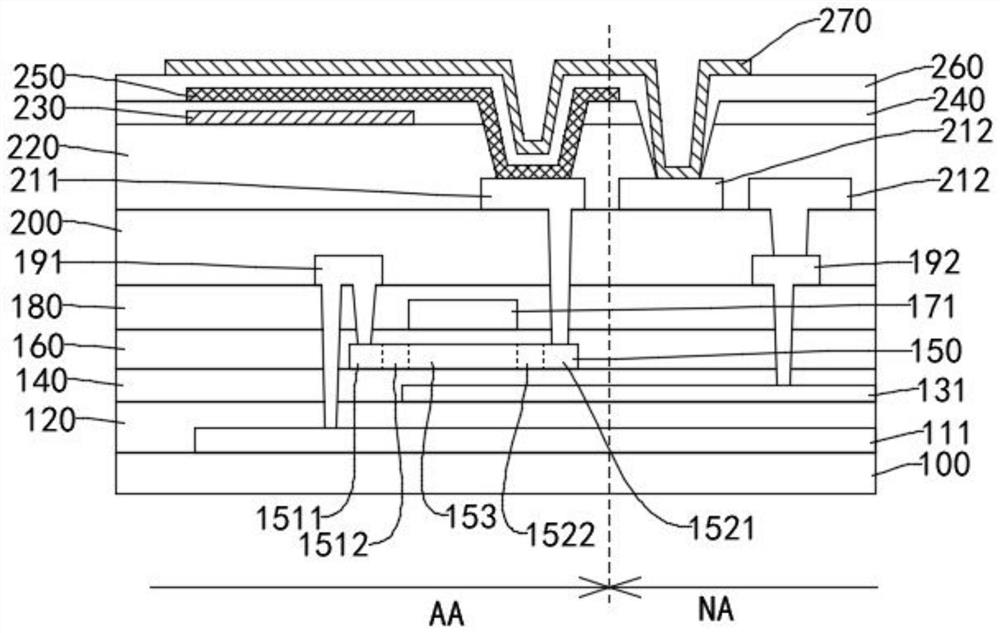
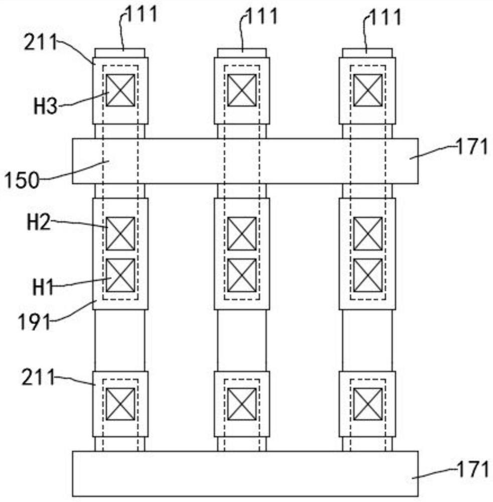
[0028] An embodiment of the present application provides a display panel, the display panel includes a first conductive layer disposed on one side of a substrate, an active layer disposed on a side of the first conductive layer away from the substrate, and a first conductive layer disposed on the active layer away from the substrate A second conductive layer on one side of the conductive layer, and a third conductive layer on the side of the second conductive layer away from the active layer, the first conductive layer includes data lines, and the active layer includes source contacts The second conductive layer includes a scan line, and the third conductive layer includes a first connection body, and the first connection body is electrically connected to the source contact portion and the data line. In the display panel provided by the embodiment of the present application, the first connecting body and the data line are respectively disposed in the upper and lower opposite layers of the active layer, and the first connecting body and the scanning line are disposed on different conductive film layers of the display panel. , it is beneficial to realize the overlapping arrangement of the active layer and the data line, reduce the occupied space of the active layer and its corresponding thin film transistor, and realize the improvement of the pixel density of the display panel; and because the first connecting body and the scanning line are located in different conductive films In the layer, the first connector can extend to the wiring area of ​​the scan line, thereby completely covering the connection hole between the first connector and the active layer, preventing the active layer from being damaged during the etching process, and improving the process yield.
[0029] The related technical features of the display panel provided by the embodiments of the present application will be described below with reference to the accompanying drawings. see figure 1 and figure 2 , figure 1 is a schematic diagram of a partial cross-sectional structure of the display panel provided by the embodiment of the present application, figure 2 It is a partial perspective view of the display panel provided by the embodiment of the present application.
[0030] This embodiment provides a display panel, the display panel includes: a substrate 100; a first conductive layer disposed on one side of the substrate 100, the first conductive layer including data lines 111; disposed on the first conductive layer The active layer 150 on the side of the layer away from the substrate 100, the active layer 150 includes a source contact, a drain contact, and a space between the source contact and the drain contact The channel portion 153, the source contact portion includes a source heavily doped region 1511 and a source lightly doped region 1512, the drain contact portion includes a drain heavily doped region 1521 and a drain lightly doped region 1522 ; a second conductive layer disposed on the side of the active layer 150 away from the first conductive layer, and the second conductive layer includes scan lines 171; disposed on the second conductive layer away from the active layer The third conductive layer on one side of the layer 150 includes the first connecting body 191 .
[0031] Wherein, the first connecting body 191 is electrically connected to the source contact portion, specifically, is electrically connected to the source heavily doped region 1511 ; and the first connecting body 191 is also connected to the source The data line 111 is electrically connected, and at least a part of the data line 111 overlaps with the active layer 150 . The data signal transmitted by the data line 111 is transmitted to the source contact through the first connection body 191 . In this embodiment, by arranging the first connecting body 191 and the data line 111 on the upper and lower sides of the active layer 150 respectively, it is convenient to realize the overlapping arrangement of the active layer 150 and the data line 111 and reduce the size of the active layer 150 . The space occupied by the layer 150 and its corresponding thin film transistors can improve the pixel density of the display panel; It can be extended to the wiring area of ​​the scan line 171 to shield the connection hole between the first connection body 191 and the active layer 150 and prevent the active layer 150 from being damaged by the etching solution through the connection hole during the etching process.
[0032] Further, the display panel further includes a fourth conductive layer located on a side of the third conductive layer away from the second conductive layer, the fourth conductive layer includes a second connection body 211, and the second connection The body 211 is electrically connected to the drain contact. Specifically, the second connection body 211 is electrically connected to the heavily doped drain region 1521 of the drain contact. The data signal transmitted from the first connection body 191 to the active layer 150 is transmitted to the second connection body 211 through the source contact portion, the channel portion 153 and the drain contact portion. It can be understood that in this embodiment, the second connecting body 211 and the first connecting body 191 are arranged in different conductive film layers, which is beneficial to realize the connection between the first connecting body 191 and the second connecting body 211 The side of the first connection body 191 is fully expanded, and it is beneficial to fully expand the second connection body 211 to the side of the first connection body 191, so as to ensure that the first connection body 191 and the second connection body 211 have sufficient At the same time, it ensures that the interval span between the first connecting body 191 and the second connecting body 211 is minimized, thereby reducing the space occupied by the corresponding thin film transistors and improving the pixel density of the display panel.
[0033] Specifically, please continue to refer to figure 1 and figure 2, in this embodiment, the display panel has a display area AA and a non-display area NA adjacent to the display area AA; the display area AA corresponds to an area in the display panel that has a display screen function; the non-display area AA The display area NA can be the border area of ​​the display panel, or the area that is bent to the back of the display panel through the bending portion, and a variety of signal lines, driving circuits, thin film transistor devices, etc. are arranged in the non-display area NA. , and part of the film structure is the same or similar to the film structure in the display area AA of the display panel.
[0034] The display panel further includes: a buffer layer 120 disposed on the substrate 100 and covering the first conductive layer; a fifth conductive layer disposed on the buffer layer 120, the fifth conductive layer including shielding Line 131, the fifth conductive layer is partially disposed in the non-display area NA; the first insulating layer 140 disposed on the buffer layer 120 and covering the fifth conductive layer, the active layer 150 is provided on the first insulating layer 140; a second insulating layer 160 is provided on the first insulating layer 140 and covers the active layer 150, and the second conductive layer is provided on the second insulating layer 160; a third insulating layer 180 disposed on the second insulating layer 160 and covering the second conductive layer, the third conductive layer being disposed on the third insulating layer 180; disposed on the first The fourth insulating layer 200 on the three insulating layers 180 and covering the third conductive layer is disposed on the fourth insulating layer 200 .
[0035] Wherein, the substrate 100 may be a glass substrate or a polyimide substrate, etc.; the buffer layer 120 may include a composite structure film layer formed of silicon nitride, silicon oxide, etc.; the first insulating layer 140, the The second insulating layer 160, the third insulating layer 180 and the fourth insulating layer 200 may be made of insulating materials such as silicon oxide or silicon nitride; the first conductive layer, the second conductive layer, The third conductive layer, the fourth conductive layer and the fifth conductive layer may all be made of conductive metal, such as metal copper, silver, etc.; the active layer 150 may be made of a polymer semiconductor material , and the source contact portion and the drain contact portion are formed through an ion doping process.
[0036] Specifically, the first connection body 191 is electrically connected to the data line 111 through a first via hole H1 , and the first via hole H1 passes through the buffer layer 120 , the first insulating layer 140 , The holes of the second insulating layer 160 and the third insulating layer 180; the first connecting body 191 is also electrically connected to the source contact part through a second via hole H2, the second via hole H2 is a hole passing through the second insulating layer 160 and the third insulating layer 180; the second connecting body 211 is electrically connected to the drain contact part through a third via hole H3, the third The hole H3 is a hole passing through the second insulating layer 160 , the third insulating layer 180 and the fourth insulating layer 200 .
[0037] Further, in this embodiment, the active layer 150 is elongated; the extending direction of the active layer 150 is the same as the extending direction of the data line 111 , and the active layer 150 is in the The orthographic projection on the first conductive layer coincides with the data line 111 . The extending direction of the active layer 150 may refer to the length direction of the active layer 150 , and the extending direction of the data lines 111 may refer to the length direction of the data lines 111 . In this embodiment, by setting the extension direction of the active layer 150 to be the same as the extension direction of the data lines 111 , the span of the active layer 150 in the extension direction perpendicular to the data lines 111 is reduced, and the active layer is realized. The reduction of the space occupied by the thin film transistors corresponding to 150 is beneficial to reduce the distance between two adjacent data lines 111 , and to improve the pixel density and display resolution of the display panel.
[0038] Further, in the extension direction perpendicular to the data line 111, the size of the data line 111 is greater than or equal to the size of the active layer 150; or, the width of the data line 111 is greater than or equal to the active layer 150. The width of the source layer 150 . In this embodiment, the width of the data line 111 is set to be greater than or equal to the width of the active layer 150 , and the positions of the two are corresponding up and down, so as to form the shielding effect of the data line 111 on the active layer 150 and prevent the substrate 100 from being exposed to the side of the substrate 100 . The light entering the display panel affects the performance of the active layer 150 and improves the stability of the thin film transistor.
[0039] Further, the orthographic projection of the first connecting body 191 on the first conductive layer at least partially overlaps with the data line 111 , and the orthographic projection of the second connecting body 211 on the first conductive layer is the same as that of the data line 111 . The data lines 111 are at least partially overlapped. It can be understood that through the above setting, the design of the arrangement of the first connecting body 191 and the second connecting body 211 along the extending direction of the data line 111 is realized, and the active layer 150 and the first connecting body 191 are further realized. The layout features of the second connecting body 211 and the second connecting body 211 are arranged along the data line 111 , so that the corresponding thin film transistor occupies a small lateral space, which is beneficial to promote the improvement of the pixel density and resolution of the display panel.
[0040] The extending direction of the scan lines 171 may be perpendicular to the extending direction of the data lines 111 , or may form other specific angles. The scan line 171 and the active layer 150 have a cross-overlapping region in spatial layout, and the orthographic projection of the scan line 171 on the active layer 150 coincides with the channel portion 153 ; more specifically , the orthographic projection of the overlapping region of the scan line 171 and the active layer 150 on the active layer 150 coincides with the channel portion 153 .
[0041] The shielding traces 131 located in the fifth conductive layer at least cover the overlapping area of ​​the data lines 111 and the scan lines 171 , so that the shielding traces 131 at least cover the channel portion 153 . It can be understood that when the data line 111 located on one side of the active layer 150 transmits data signals, the electric field generated by the data line 111 will affect the active layer 150, causing the active layer 150 to be abnormally turned on or abnormally turned off, thereby affecting the thin film The performance of the transistor; in this embodiment, the shielding trace 131 is arranged between the data line 111 and the active layer 150 to shield the electric field generated by the data line 111 and improve the stability of the active layer 150 sex. Optionally, the shielding traces 131 are electrically connected to the common voltage traces to access the common voltage, thereby producing better signal shielding effect.
[0042] Further, the display panel further includes: a flat layer 220 disposed on the fourth insulating layer 200 and covering the fourth conductive layer, and a plurality of layers of the fourth conductive layer are disposed on the flat layer 220 A partially exposed via hole; a first common electrode 230 disposed on the flat layer 220 , the first common electrode 230 is electrically connected to a common voltage trace to access the common voltage; disposed on the flat layer 220 and cover the first passivation layer 240 of the first common electrode 230, the first passivation layer 240 is provided with via holes partially exposing the fourth conductive layer; provided on the first passivation layer The pixel electrode 250 on the 240, the pixel electrode 250 is electrically connected to the second connector 211 through the via hole on the flat layer 220 and the via hole on the first passivation layer 240, so as to receive the The data signal transmitted by the second connector 211 ; the second passivation layer 260 disposed on the first passivation layer 240 and covering the pixel electrode 250 ; the second passivation layer 260 disposed on the second passivation layer 260 The second common electrode 270, the second common electrode 270 is electrically connected to the common voltage trace to access the common voltage signal.
[0043] Optionally, the first common electrode 230 , the pixel electrode 250 and the second common electrode 270 may be made of indium tin oxide material.
[0044] It can be understood that as the size of the thin film transistor decreases, the size of its gate also decreases, and the storage capacitance in the pixel circuit corresponding to the thin film transistor will also decrease, and the reduction of the storage capacitance will lead to the function of the display panel. Abnormal; in this embodiment, the first common electrode 230 and the second common electrode 270 are respectively disposed on the upper and lower opposite sides of the pixel electrode 250 to compensate for the loss of electric field strength caused by the reduction of the storage capacitance and improve the display quality of the display panel and display stability.
[0045] Further, in the non-display area NA, the third conductive layer further includes a third connection body 192 , and the fourth conductive layer further includes a fourth connection body 212 . The third connecting body 192 is electrically connected to the shielding trace 131 through the first insulating layer 140 , the second insulating layer 160 , and the via holes on the third insulating layer 180 ; the fourth The connecting body 212 is electrically connected to the third connecting body 192 through the via hole on the fourth insulating layer 200 ; the second common electrode 270 passes through the flat layer 220 , the first passivation layer 240 and the The via hole on the second passivation layer 260 is electrically connected to the fourth connection body 212 ; and then the second common electrode 270 , the fourth connection body 212 , the third connection body 192 and all The shielded traces 131 are all electrically connected to the common voltage traces.
[0046] Optionally, the display panel may be a liquid crystal display panel, and the display panel further includes: a liquid crystal layer located on the side of the second common electrode 270 away from the second passivation layer 260 , and the liquid crystal layer is inside the liquid crystal layer. A liquid crystal is provided; and an opposite substrate located on the side of the liquid crystal layer away from the second common electrode 270, a color resist layer may be provided in the opposite substrate, and the color resist layer includes a color resist corresponding to each pixel unit. resistance.
[0047] To sum up, the display panel provided in this embodiment includes a first conductive layer and a second conductive layer disposed on opposite sides of the active layer 150 , and a second conductive layer located on the second conductive layer away from the active layer 150 . The third conductive layer on the side of layer 150, the first conductive layer includes data lines 111, the active layer 150 includes source contacts, the second conductive layer includes scan lines 171, the third conductive layer A first connecting body 191 is included, and the first connecting body 191 is electrically connected to the source contact portion and the data line 111 . In this embodiment, by disposing the first connecting body 191 and the data line 111 in the upper and lower opposite layers of the active layer 150 respectively, and disposing the first connecting body 191 and the scanning line 171 on different conductive film layers of the display panel, It is beneficial to realize the overlapping arrangement of the active layer 150 and the data line 111, reduce the occupied space of the active layer 150 and its corresponding thin film transistor, and realize the improvement of the pixel density of the display panel; Located in different conductive film layers, so that the first connecting body 191 can extend to the wiring area of ​​the scan line 171, so as to completely cover the connecting hole between the first connecting body 191 and the active layer 150, preventing the etching process from damaging the active layer 150, thereby improving the process yield.
[0048] It should be noted that although the present application discloses the above with specific embodiments, the above-mentioned embodiments are not intended to limit the present application. Those of ordinary skill in the art can make various modifications without departing from the spirit and scope of the present application. Therefore, the scope of protection of this application is subject to the scope defined by the claims.

PUM

no PUM

Description & Claims & Application Information

We can also present the details of the Description, Claims and Application information to help users get a comprehensive understanding of the technical details of the patent, such as background art, summary of invention, brief description of drawings, description of embodiments, and other original content. On the other hand, users can also determine the specific scope of protection of the technology through the list of claims; as well as understand the changes in the life cycle of the technology with the presentation of the patent timeline. Login to view more.

Similar technology patents

Betel nut packing machine

ActiveCN105270678ASmall footprintreduce noise
Owner:KUNSHAN BAIAO INTELLIGENT EQUIP CO LTD

Electric heater for air conditioner indoor unit

Owner:GREE ELECTRIC APPLIANCES INC OF ZHUHAI

Portable wetlands

InactiveUS20080179240A1high surface areasmall footprint
Owner:KAUPPI FREDERICK J +2

Classification and recommendation of technical efficacy words

Why Eureka
Try Eureka