Supercharge Your Innovation With Domain-Expert AI Agents!

Flexible circuit board bonding pad windowing manufacturing process using flexible ink

A flexible circuit board and manufacturing process technology, applied in the direction of printed circuit manufacturing, assembling printed circuits with electrical components, printed circuits, etc. effect of ability

Inactive Publication Date: 2022-07-01
信丰迅捷兴电路科技有限公司
View PDF8 Cites 0 Cited by
  • Summary
  • Abstract
  • Description
  • Claims
  • Application Information

AI Technical Summary

Problems solved by technology

[0004] In this processing process, exposure alignment deviation and film expansion and contraction tolerance are the keys to affect the precision of pad window opening. At the same time, development is to remove unpolymerized ink during exposure through 40%-60% sodium carbonate. In this chemical The side erosion effect of 1.5mil on one side will be produced in the process of potion, and there is a risk of falling off the bridge when the solder bridge between IC and IC is less than 4mil, so that there will be a short circuit phenomenon in the soldering process of packaging IC. Therefore, use The flexible ink process is also unable to adapt to the production of all small-pitch FPC circuit boards
[0005] With the miniaturization and thinning of electronic devices, the required printed circuit boards are becoming more and more precise. In FPC circuit boards, the surface insulation layer is protected by polyimide cover film or flexible photosensitive ink; however, Due to the limitations of the two technologies and processing capabilities, traditional processing methods are no longer suitable for the production of such products in dense window-opening and patching areas and IC packaging FPC circuit boards.

Method used


Image

  • Flexible circuit board bonding pad windowing manufacturing process using flexible ink
  • Flexible circuit board bonding pad windowing manufacturing process using flexible ink
  • Flexible circuit board bonding pad windowing manufacturing process using flexible ink

Examples


Embodiment Construction

[0037] Next, combine Figure 1-3 A specific embodiment of the present invention is described in detail.

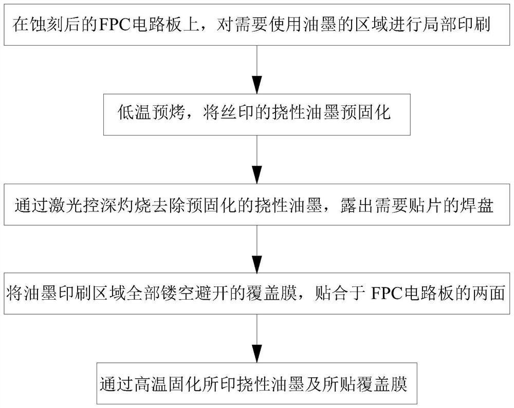
[0038] Reference attached figure 1 , a flexible circuit board pad window manufacturing process using flexible ink, comprising the following steps:

[0039] Step 1, print solder mask, and perform partial printing on the area where ink needs to be used on the etched FPC circuit board;

[0040] Step 2, curing, pre-curing the silk-screened flexible ink by pre-baking at a low temperature;

[0041] Step 3, laser control depth, remove the pre-cured flexible ink by laser control depth burning, and expose the pads that need to be patched;

[0042] Step 4, paste the cover film, and attach the cover film that is avoided by hollowing out all the ink printing area, and attach it to both sides of the FPC circuit board;

[0043] Step 5, curing, the printed flexible ink and the attached cover film are cured by high temperature.

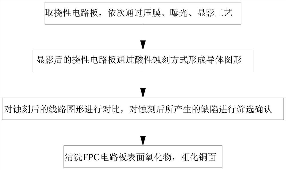
[0044] Reference attached figure 2 , before step 1, ...


PUM

PropertyMeasurementUnit
thicknessaaaaaaaaaa

Abstract

A flexible circuit board bonding pad windowing manufacturing process using flexible ink comprises the following steps of: printing a solder mask, and locally printing an area needing to use ink on an etched FPC (Flexible Printed Circuit); curing: pre-curing the flexible ink subjected to silk-screen printing through low-temperature pre-baking; laser depth control is carried out, the pre-cured flexible ink is removed through laser depth control burning, a bonding pad needing to be pasted is exposed, and then windowing is carried out; covering film pasting, wherein the covering film away from the ink printing area is completely hollowed out, and the covering film is pasted to the two faces of the FPC circuit board; and curing, namely curing the printed flexible ink and the attached cover film at high temperature. According to the hardness difference between the ink and copper, the flexible ink is cut through laser in a depth-controlled mode to achieve the purpose of windowing, and the integrity of the bonding pad can be guaranteed while the ink is removed; the method is mainly suitable for the circuit board in a small-spacing dense bonding pad windowing area, and solves the technical problem that the traditional covering film and ink process cannot meet the requirement of precise FPC circuit board processing.

Description

technical field [0001] The invention relates to the field of printed circuit board technology, in particular to a process for making a window of a flexible circuit board pad using flexible ink. The burning window method solves the problem of insufficient spacing between the window covering film and the ink in the precision solder joint area, and improves the application of flexible circuit boards and rigid-flex circuit boards in high-density, small-package devices. Background technique [0002] Like the rigid-flex circuit board, the flexible circuit board has the characteristics of three-dimensional installation. In the flexible circuit board, the surface of the conductor is protected by an insulating cover film. Before the surface cover film is attached, the welding area of ​​the pad will be opened with a machine or a laser, and then the cover film will be opened manually or by automatic equipment. The cover film after opening the window is attached to the surface of the F...

Claims


Application Information

Patent Timeline
Patent Type & Authority Applications(China)
IPC IPC(8): H05K3/02H05K3/34H05K3/24
CPCH05K3/02H05K3/341H05K3/245H05K2203/0228
Inventor 陈定成邓建伟龙小虎
Owner 信丰迅捷兴电路科技有限公司
Features
  • R&D
  • Intellectual Property
  • Life Sciences
  • Materials
  • Tech Scout
  • Unparalleled Data Quality
  • Higher Quality Content
  • 60% Fewer Hallucinations
Learn More