Groove silicon carbide MPS diode structure and preparation method thereof

A silicon carbide and diode technology, applied in the field of trench silicon carbide MPS diode structure and preparation, can solve the problems of not being able to further improve the anti-surge capability of the device, and cannot further reduce the forward conduction voltage drop of the device, so as to reduce the forward conduction Effect of pressure drop, increase in area, increase in area

Pending Publication Date: 2022-07-08
CHINA ZHENHUA GRP YONGGUANG ELECTRONICS CO LTD STATE OWNED NO 873 FACTORY
View PDF1 Cites 0 Cited by
  • Summary
  • Abstract
  • Description
  • Claims
  • Application Information

AI Technical Summary

Problems solved by technology

[0003] The disadvantage of the existing structure is that in the MPS structure of the planar structure, on the one hand, the area of ​​the ohmic contact area formed by the contact interface between the P+ implantation region 13 and the metal 12 above it is limited by the planar area, and there is a problem that the anti-surge capability of the device cannot be further improved; On the

Method used


Image

  • Groove silicon carbide MPS diode structure and preparation method thereof
  • Groove silicon carbide MPS diode structure and preparation method thereof
  • Groove silicon carbide MPS diode structure and preparation method thereof

Examples


Example Embodiment

[0055] The technical solutions of the present invention are further described below, but the claimed scope is not limited to the description.

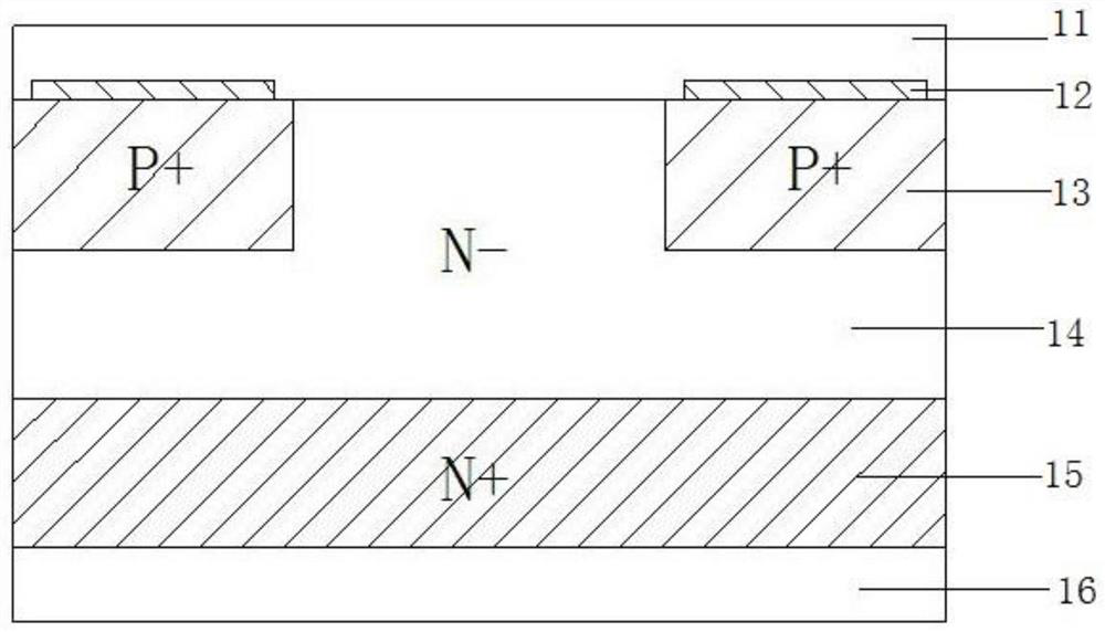
[0056] The present invention provides a trench silicon carbide MPS diode structure, comprising:

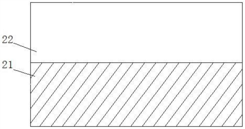
[0057] Silicon carbide N+ substrate 21 providing the substrate basis;

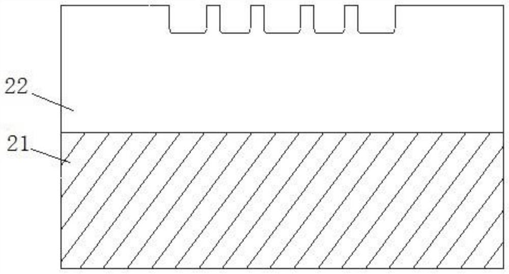
[0058] The silicon carbide epitaxial layer 22 located above the silicon carbide N+ substrate 21, the thickness of the silicon carbide epitaxial layer 22 is 5-20 μm;

[0059] A plurality of P+ field limiting rings 23 are located in the silicon carbide epitaxial layer 22 at intervals. The silicon carbide epitaxial layer 22 has grooves with a depth of 0.4 μm to 1.2 μm and a width of 1 μm to 5 μm to cooperate with the P+ field limiting rings 23 ;

[0060] The P+ trench region 24 is located in the periodically arranged silicon carbide epitaxial layer 22. The silicon carbide epitaxial layer 22 is periodically arranged with trenches. The depth of the trenches of the silicon...


PUM

PropertyMeasurementUnit
Resistivityaaaaaaaaaa
Thicknessaaaaaaaaaa
Thicknessaaaaaaaaaa

Abstract

The invention discloses a groove silicon carbide MPS diode structure and a preparation method thereof, and the structure comprises the components of silicon carbide ohmic contact metal which is located on a P + groove region and is matched with a groove; the silicon carbide Schottky contact metal is positioned above the silicon carbide epitaxial layer and the silicon carbide ohmic contact metal and is in groove fit with the silicon carbide epitaxial layer and the silicon carbide ohmic contact metal; a groove matching structure of the silicon carbide Schottky contact metal and the silicon carbide epitaxial layer interface Schottky contact region can effectively increase the area of the Schottky contact region, so that the forward conduction voltage drop of the device is effectively further reduced, and the current density of the device is increased; and the area of the ohmic contact region is increased by a groove-groove matching structure of the P + groove region and the ohmic contact region of the silicon carbide ohmic contact metal interface, so that higher current can pass through the device in a surge mode, and the anti-surge performance of the device is further improved.

Description

technical field [0001] The invention relates to a trench silicon carbide MPS diode structure and a preparation method, and belongs to the technical field of electronic components. Background technique [0002] Prior art silicon carbide MPS diodes (also called integrated PIN Schottky diodes) such as figure 1 As shown, its main structure includes: metal upper electrode 11; silicon carbide ohmic contact metal 12 under the metal upper electrode 11; silicon carbide P+ implantation region 13 under the ohmic contact metal, wherein the P+ implantation region 13 and the metal above it 12 The contact interface is an ohmic contact area; the silicon carbide N-type epitaxial layer 14 including the implanted region 13, wherein the contact interface between the silicon carbide epitaxial layer 14 and the metal upper electrode 11 is a Schottky contact area; Silicon carbide substrate 15, metal lower electrode 16 located under the silicon carbide epitaxial layer; its main structure is also di...

Claims


Application Information

Patent Timeline
IPC IPC(8): H01L29/06H01L29/872H01L21/329
CPCH01L29/0684H01L29/872H01L29/6606
Inventor 孟繁新陆超袁强贺晓金王海锐王博余文兴张浩宇何静
Owner CHINA ZHENHUA GRP YONGGUANG ELECTRONICS CO LTD STATE OWNED NO 873 FACTORY
Why Eureka
Try Eureka