Novel packaging structure and manufacturing method thereof

A packaging structure and a new type of technology, applied in semiconductor/solid-state device manufacturing, semiconductor devices, electrical components, etc., can solve the problems of decreased welding push-pull force, affecting the reliability of CSP packaged devices, etc. The effect of simple technical methods

Pending Publication Date: 2022-07-12
HAIDIKE NANTONG OPTOELECTRONICS TECH CO LTD
View PDF0 Cites 0 Cited by
  • Summary
  • Abstract
  • Description
  • Claims
  • Application Information

AI Technical Summary

Problems solved by technology

However, the conventional CSP light source technology often cuts the wafer into pieces, sorts and rearranges the light-emitting chips, and then performs follow-up processes such as phosphor powder or fluorescent colloid laminating and spraying. The bottom surface of the electrode of the chip is on the same plane. Such a package structure will lead to a decrease in the welding push-pull force during the subsequent CSP package mounting process, which will seriously affect the reliability of the CSP package device.

Method used


Image

  • Novel packaging structure and manufacturing method thereof
  • Novel packaging structure and manufacturing method thereof
  • Novel packaging structure and manufacturing method thereof

Examples


Embodiment 1

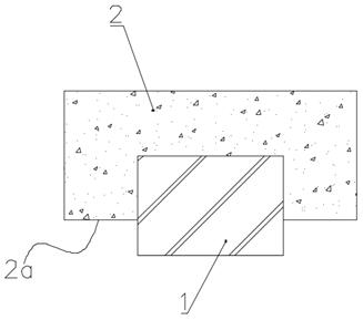
[0037] like figure 1 As shown, the novel packaging structure of the present invention includes a chip 1, which can be a positive chip or a flip chip. The outer surface of the chip 1 is covered with an outer packaging layer 2, and the outer packaging layer 2 includes an outer packaging layer arranged on the chip. 1. The top encapsulation layer on the top surface and the side encapsulation layer disposed on the side of the chip, wherein the bottom surface 2a of the side encapsulation layer on at least one side is 2 μm higher than the bottom surface of the chip 1 and not higher than half of the height of the chip 1 .

[0038] The comparison between the package structure in the first embodiment of the present invention and the traditional package structure soldered to the substrate is as follows:

[0039] Traditional CSP packaging structure: the adopted chip specifications are 760 μm long, 330 μm wide, 150 μm high, the top packaging layer thickness of the outer packaging layer is ...

Embodiment 2

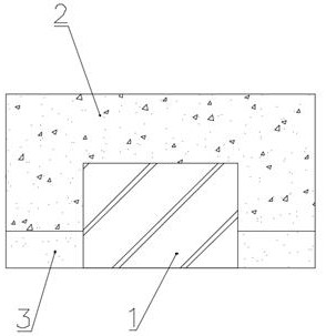
[0045] figure 2 Another structure of the packaging structure of the present invention is shown, which includes a chip 1, and a sacrificial layer 3 close to the side wall of the chip 1 is provided at the bottom periphery of the chip 1, and the height of the sacrificial layer 3 is not higher than half of the height of the chip. , the bottom surface of the sacrificial layer 3 is flush with the bottom surface of the chip 1 or lower than the bottom surface of the chip. As a more specific implementation of this embodiment, the thickness of the sacrificial layer 3 is not limited to be uniform, and it can gradually decrease from the center of the chip 1 to the outside.

[0046] An outer encapsulation layer 2 covering the outer surface of the chip 1 is provided on the upper surface of the sacrificial layer 3. The outer encapsulation layer 2 includes a top encapsulation layer arranged on the top surface of the chip 1 and a side encapsulation layer arranged on the side of the chip. The...

Embodiment 3

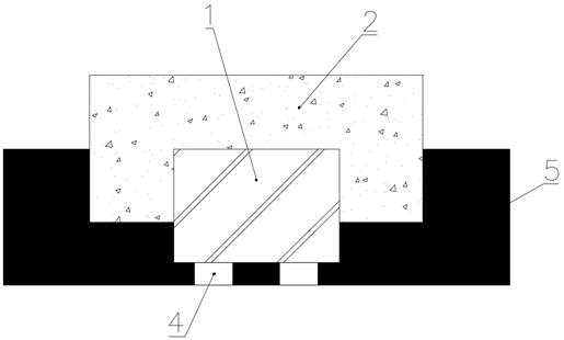
[0048] like image 3 As shown, in this embodiment, a chip 1 is included, the outer surface of the chip 1 is covered with an outer packaging layer 2, and the outer packaging layer 2 includes a top packaging layer arranged on the top surface of the chip 1 and a side packaging layer arranged on the side of the chip. layer, wherein the bottom surface 2a of the side encapsulation layer is not lower than the bottom surface of the chip 1 by 2 μm, and is not higher than half of the height of the chip 1 .

[0049] In this embodiment, the bottom surface of the chip 1 is provided with an electrode 4 that protrudes downward from the bottom surface, the bottom surface and the side surface of the outer packaging layer 2 and the bottom surface and the bottom surface of the chip are covered with a reflective layer 5, and the center bottom of the reflective layer 5 has two Electrode channel with exposed electrodes. The upper surface of the reflective layer is not higher than the upper surface...


PUM

PropertyMeasurementUnit
thicknessaaaaaaaaaa

Abstract

The invention relates to a novel packaging structure and a manufacturing method thereof, the novel packaging structure comprises a chip, the outer surface of the chip is coated with an outer packaging layer, the outer packaging layer comprises a top packaging layer arranged on the top surface of the chip and a side packaging layer arranged on the side surface of the chip, and the novel packaging structure is characterized in that the bottom surface of the side packaging layer is higher than the bottom surface of the chip. The packaging structure has the advantages that the bottom surface of the side packaging layer, located on the side surface of the chip, in the outer packaging layer is 2 microns higher than the bottom surface of the chip, during chip welding, due to the fact that no other materials exist on the periphery of the bottom surface of the chip, molten solder paste can be better connected with the substrate to be combined with the chip, push-pull force is not affected after welding, and the chip is not prone to falling off.

Description

technical field [0001] The invention relates to an LED package structure, in particular to a novel package structure with high push-pull force after welding, and a manufacturing method of the package structure. Background technique [0002] Chip Scale Package (CSP, Chip Scale Package), this packaging method came into being based on the development of flip-chip technology in recent years, and commercialized mass production after 2015. For details on the development of packaging technology, please refer to the literature: Wang Jietian, Current Situation and Development of LED Packaging Technology [J], Science and Technology Innovation and Application, 2017(12):42. [0003] CSP light source refers to a class of LED devices using CSP packaging technology. The core of the CSP light source is that the CSP light source uses phosphor powder or fluorescent colloid film to wrap the flip-chip structure, eliminating most of the packaging steps and structures of traditional LED light sou...

Claims


Application Information

Patent Timeline
Patent Type & Authority Applications(China)
IPC IPC(8): H01L27/15H01L21/78H01L33/54H01L33/60
CPCH01L27/156H01L21/78H01L33/54H01L33/60
Inventor 孙智江王书昶吴陆
Owner HAIDIKE NANTONG OPTOELECTRONICS TECH CO LTD
Why Eureka
Try Eureka