MiniLED chip and manufacturing method thereof

A manufacturing method and chip technology, applied to semiconductor devices, electrical components, circuits, etc., can solve problems such as limited heat dissipation area, offset of photoelectric parameters, weakened heat dissipation capacity of chips, etc., to achieve good heat dissipation effect, good reliability, and lower temperature Effect

Active Publication Date: 2022-07-15
南昌凯捷半导体科技有限公司
View PDF6 Cites 1 Cited by
  • Summary
  • Abstract
  • Description
  • Claims
  • Application Information

AI Technical Summary

Problems solved by technology

Due to the small size of the mini LED chip, the heat dissipation area is limited, and the current mini LED chip needs to grow a thicker passivation layer of silicon dioxide to cover the surface of the chip during the production process to ensure that the chip can work normally, which further improves the heat dissipation capacity of the chip. weaken
At the same time, when the mini LED chip is working, the temperature of the whole chip will rise significantly, causing the photoelectric parameters to shift; while the mini LED chip will work at high temperature for a long time, it will cause irreversible damage to the light-emitting layer, which will seriously affect chip lifetime

Method used


Image

  • MiniLED chip and manufacturing method thereof
  • MiniLED chip and manufacturing method thereof
  • MiniLED chip and manufacturing method thereof

Examples


Embodiment Construction

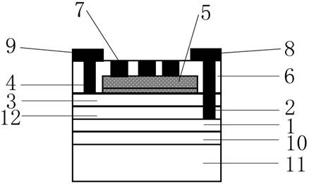
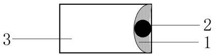
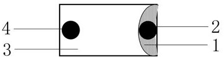
[0045] The technical solutions in the embodiments of the present application will be clearly and completely described below with reference to the drawings in the embodiments of the present application. Obviously, the described embodiments are only a part of the embodiments of the present application, but not all of the embodiments. The following description of at least one exemplary embodiment is merely illustrative in nature and in no way limits the application, its application, or uses in any way. Based on the embodiments in this application, all other embodiments obtained by those of ordinary skill in the art without creative work fall within the protection scope of this application.

[0046] In the description of this application, it should be understood that the use of words such as "first" and "second" to define components is only for the convenience of distinguishing corresponding components. Unless otherwise stated, the above words have no special Therefore, it cannot ...


PUM

PropertyMeasurementUnit
thicknessaaaaaaaaaa
thicknessaaaaaaaaaa
thicknessaaaaaaaaaa

Abstract

The invention relates to the technical field of LEDs, in particular to a mini LED chip and a manufacturing method thereof.The chip comprises a sapphire substrate, a bonding layer, a P-type semiconductor layer, a light-emitting layer, an N-type semiconductor layer, a P contact electrode, an N contact electrode, a graphite heat conduction layer, a passivation layer, a P electrode and an N electrode; the graphite heat conduction layer is composed of titanium oxide and graphite. Heat dissipation holes penetrating through the passivation layer are designed in the surface, corresponding to the graphite heat conduction layer, of the passivation layer, and the heat dissipation holes are backfilled with graphite and make contact with the graphite heat conduction layer. The graphite heat conduction layer is added in the mini LED chip, the heat dissipation holes are designed in the surface of the passivation layer, the heat dissipation holes are backfilled with the graphite, heat generated when the mini LED chip works can be effectively conducted out by means of the ultra-strong heat conduction capacity of the graphite, the temperature of the chip is reduced, the stability of the photoelectric property of the chip is improved, and the service life of the chip is effectively prolonged.

Description

technical field [0001] The invention relates to the technical field of LEDs, in particular to a miniLED chip and a manufacturing method thereof. Background technique [0002] Mini LED is also a mini light-emitting diode. Compared with ordinary LED display, mini LED display has higher density per unit area and smaller unit size of light source, which can bring higher brightness and controllable color gamut. Due to the small size of the mini LED chip, the heat dissipation area is limited, and the current mini LED chip needs to grow a thicker passivation layer of silicon dioxide to cover the surface of the chip during the production process to ensure that the chip can work normally, which further improves the heat dissipation capability of the chip. weaken. At the same time, when the mini LED chip is working, the temperature of the entire chip will increase significantly, causing the optoelectronic parameters to shift; while the mini LED chip works at high temperature for a lo...

Claims


Application Information

Patent Timeline
Patent Type & Authority Applications(China)
IPC IPC(8): H01L33/64H01L33/00
CPCH01L33/641H01L33/642H01L33/0066H01L2933/0075
Inventor 王克来李俊承陈宝戴文潘彬王向武
Owner 南昌凯捷半导体科技有限公司
Why Eureka
Try Eureka