Wafer-level system packaging structure and packaging method

A system packaging and wafer-level technology, applied in the direction of microstructure devices, manufacturing microstructure devices, microstructure technology, etc., can solve the problems of low packaging efficiency, save time, prevent lateral overflow, and enhance mechanical strength.

Inactive Publication Date: 2022-07-29
NINGBO SEMICON INT CORP
View PDF0 Cites 0 Cited by
  • Summary
  • Abstract
  • Description
  • Claims
  • Application Information

AI Technical Summary

Problems solved by technology

[0006] The invention discloses a wafer-level system packaging structure...

Method used


Image

  • Wafer-level system packaging structure and packaging method
  • Wafer-level system packaging structure and packaging method
  • Wafer-level system packaging structure and packaging method

Examples


Embodiment 1

[0036] This embodiment provides a wafer-level system packaging method, including the following steps:

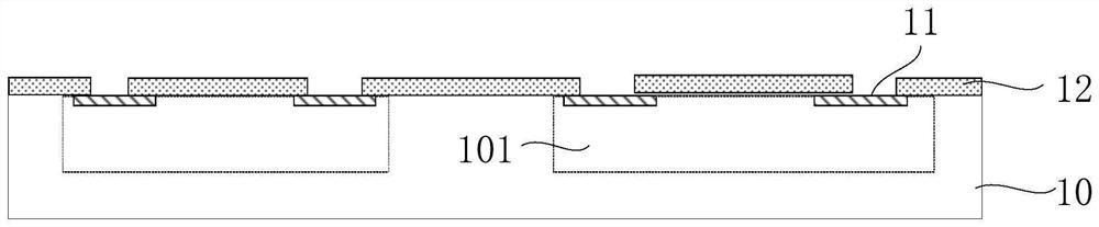
[0037] S01: Provide a first device wafer, a plurality of device modules are formed inside the first device wafer, the first device wafer has a front surface and a back surface, the front surface is exposed to electrically connect the device modules and is recessed in a plurality of first solder pads on the front side;

[0038] S02: providing a plurality of first chips, the lower surfaces of the first chips have second pads;

[0039] S03: forming an adhesive layer on the front surface of the first device wafer or the lower surface of the first chip, and forming an opening in the adhesive layer; bonding the first device through the adhesive layer the wafer and the first chip, the cavity formed by the opening is used as the working cavity of the first device module and / or the first chip; The pads are relatively surrounded by a gap;

[0040] S04: Use an electroplating process t...

Embodiment 2

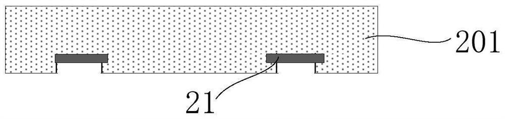
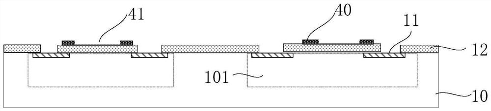
[0069] refer to Image 6 , the difference between this embodiment and Embodiment 1 is that the backside of the second chip has the first electrical connection structure 22 , the method further includes, providing a second chip 50 or a second device wafer, and connecting the second chip 50 Or the second device wafer is electrically connected to the first electrical connection structure 22 .

[0070] In the present embodiment, the first electrical connection structure 22 is formed on the back of the second chip 50 . After bonding the first chip 201 , the second chip 50 is provided; and then the second chip 50 and the first chip 201 are bonded. The second chip 50 may be electrically connected to one device module 101 , or may be electrically connected to two or more device modules 101 . The figure shows a case where the second chip 50 is electrically connected to one device module 101 . It should be noted that, for the electrical connection between the second chip 50 and the de...

Embodiment 3

[0073] refer to Figure 7 The difference between this embodiment and Embodiment 2 is that the lower surface of the first device wafer 10 has a second electrical connection structure 13, and the method further includes: providing a third chip or a third device wafer 100, The third chip or the third device wafer 100 is electrically connected to the second electrical connection structure 13 .

[0074] The lower surface of the first device wafer 10 has a second electrical connection structure 13 , the third device wafer 100 includes a plurality of third chips 51 , and the second electrical connection structure 13 is electrically connected to the third chips 51 . First, the lower surface of the first device wafer 10 is thinned to expose the second electrical connection structure 13 , and then the third device wafer 100 is bonded on the first device wafer 10 , and the third chip 51 and the For the electrical connection of the second electrical connection structure 13 , reference ma...


PUM

PropertyMeasurementUnit
Thicknessaaaaaaaaaa
Heightaaaaaaaaaa
Areaaaaaaaaaaa

Abstract

The invention provides a wafer-level system packaging structure and method, and the method comprises the steps: providing a first device wafer which is internally provided with a plurality of device modules, and is provided with a front surface and a back surface, a plurality of first welding pads which are electrically connected with the device module and are sunken in the front surface are exposed out of the front surface; providing a plurality of first chips, wherein the lower surfaces of the first chips are provided with second welding pads; forming a bonding layer on the front surface of the first device wafer or the lower surface of the first chip, and forming an opening in the bonding layer; bonding the first device wafer and the first chip through the bonding layer, and enabling a cavity formed by the opening to serve as a working cavity of the first device module and/or the first chip; the first welding pad and the second welding pad are oppositely enclosed to form a gap; and forming a conductive bump in the gap by adopting an electroplating process so as to electrically connect the first welding pad and the second welding pad.

Description

technical field [0001] The invention relates to the field of semiconductor packaging, in particular to a wafer-level system packaging structure and packaging method. Background technique [0002] System-in-package uses any combination to combine multiple active components / devices, passive components / devices, MEMS devices, discrete KGD (Known Good Die) with different functions and prepared by different processes, such as optoelectronic chips, biochips, etc., It is integrated and assembled in three dimensions (X direction, Y direction and Z direction) into a single standard package with a multi-layer device structure and can provide multiple functions to form a system or subsystem. [0003] Flip-chip (FC, Flip-Chip) soldering is a commonly used system-in-package method at present. The system-in-package method includes: providing a PCB circuit board, wherein solder balls arranged according to certain requirements are formed on the PCB circuit board (formed by a ball-mounting p...

Claims


Application Information

Patent Timeline
IPC IPC(8): H01L21/60H01L23/488B81B7/00B81B7/02B81C1/00
CPCH01L24/82H01L24/81H01L24/16B81C1/00095B81C1/00261B81B7/0006B81B7/0032B81B7/02H01L2224/16148H01L2224/18H01L2224/16225
Inventor 黄河向阳辉刘孟彬
Owner NINGBO SEMICON INT CORP
Why Eureka
Try Eureka