Monolithic integrated three-primary-color Micro-LED chip and preparation method thereof

A single-chip integration and three-color technology, applied in semiconductor devices, electrical components, nanotechnology, etc., can solve problems such as low yield, poor timeliness, and low accuracy, so as to improve crystal quality, avoid low yield, reduce The effect of small polarizing electric fields

Pending Publication Date: 2022-08-02
江苏穿越光电科技有限公司
View PDF0 Cites 0 Cited by
  • Summary
  • Abstract
  • Description
  • Claims
  • Application Information

AI Technical Summary

Problems solved by technology

[0004] The present invention provides a monolithic integrated three-primary-color Micro-LED chip and a preparation method thereof to solve the problem of low yield rate, poor timeliness, and poor timeliness in the process of preparing a Micro-LED chip array by mass transfer of a single three-primary-color Micro-LED in the prior art. The problem of low accuracy

Method used


Image

  • Monolithic integrated three-primary-color Micro-LED chip and preparation method thereof
  • Monolithic integrated three-primary-color Micro-LED chip and preparation method thereof
  • Monolithic integrated three-primary-color Micro-LED chip and preparation method thereof

Examples


Embodiment 1

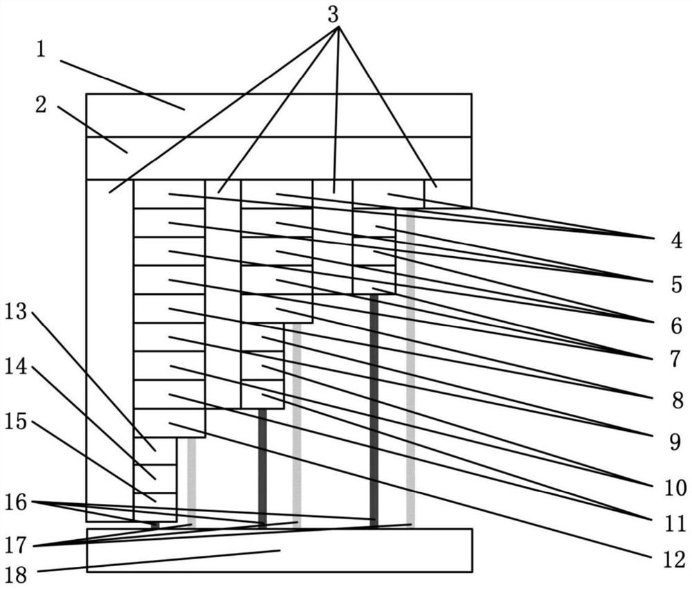
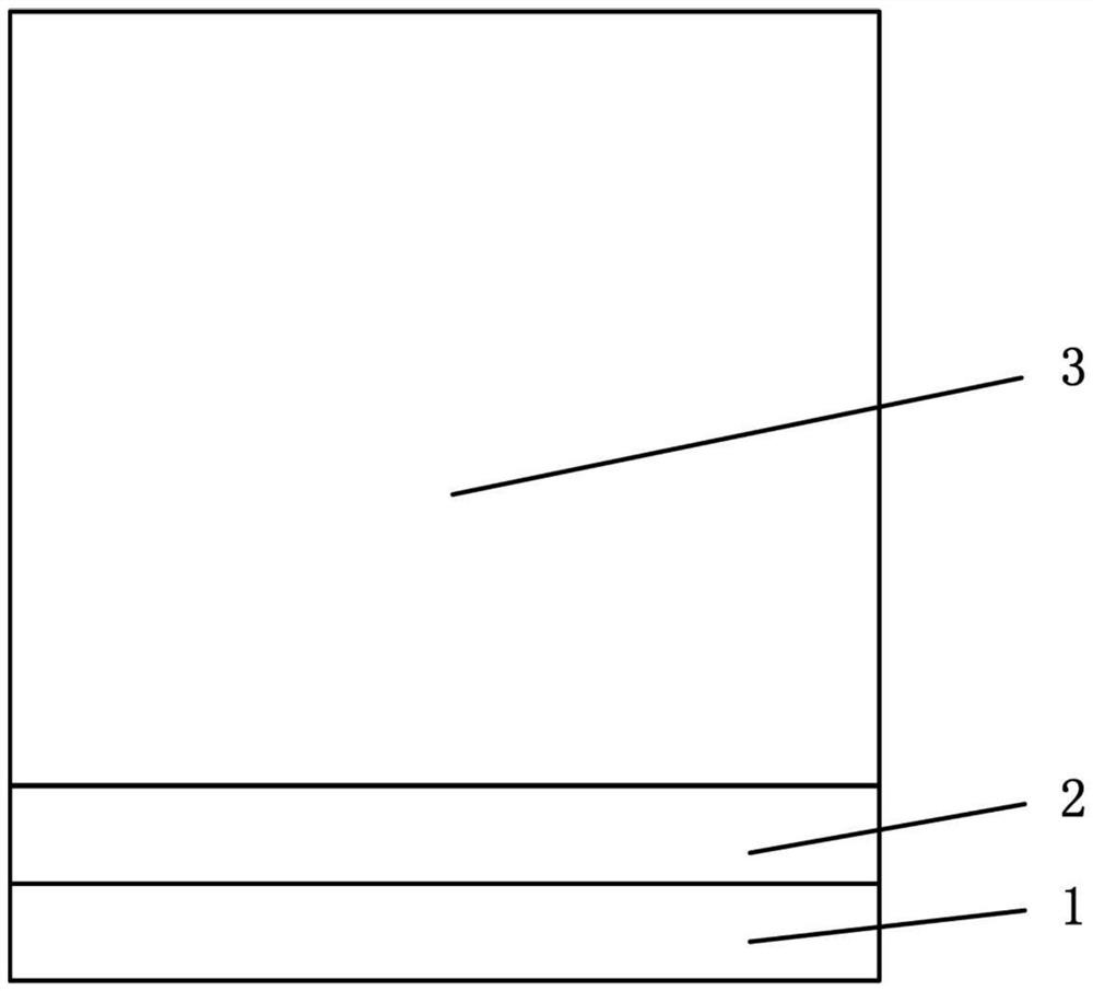
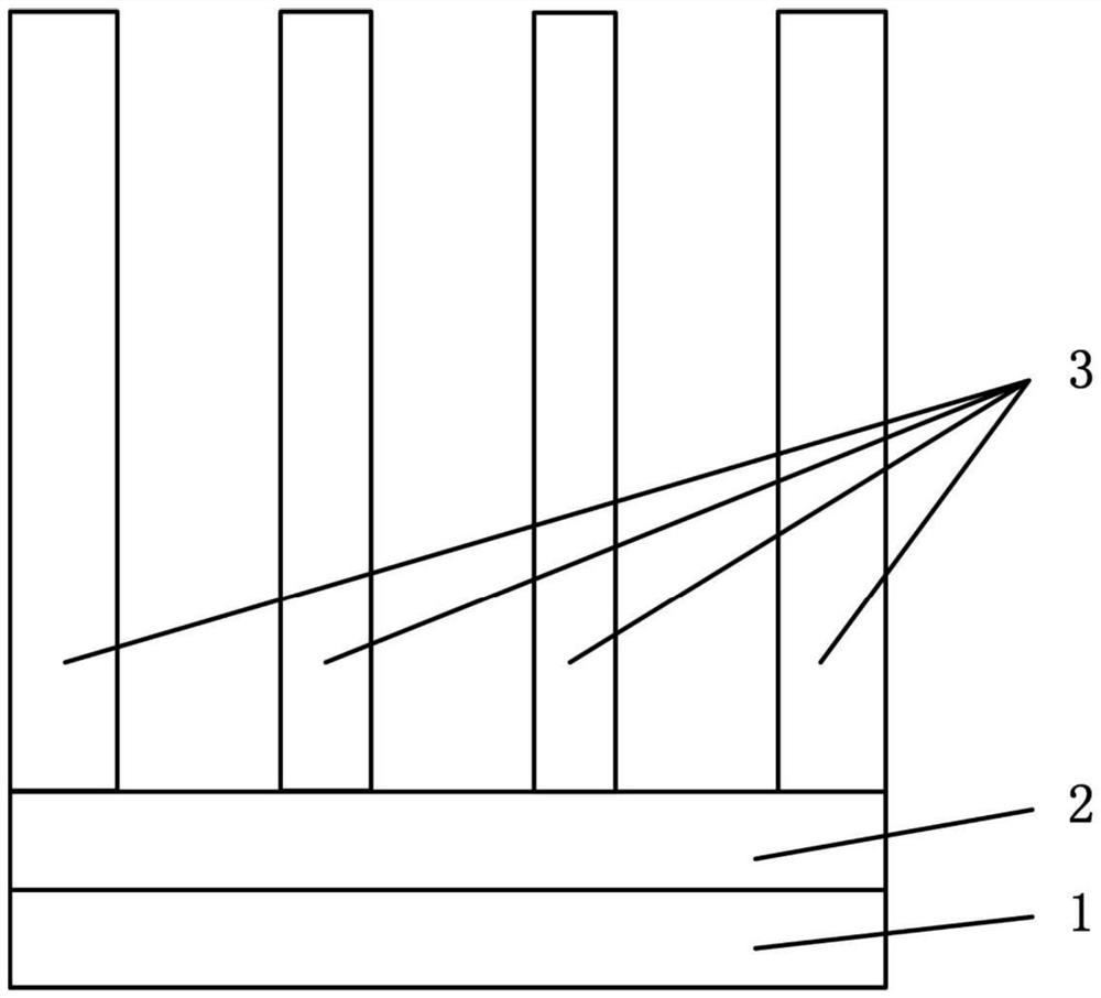
[0035] Embodiment 1 provides a monolithic integrated three-primary-color Micro-LED chip, see figure 1 , Image 6 , Figure 7 , comprising a substrate 1, a buffer layer 2 located on the substrate 1, an insulating layer 3 located on the buffer layer 2, the insulating layer 3 is etched to form a nano-scale micropore array, the micro The hole array constitutes a plurality of pixel units.

[0036] The substrate 1 can be one of sapphire, Si, and GaN, the buffer layer 2 can be a u-GaN buffer layer, and the insulating layer 3 can be SiO 2 Insulation. The thickness of the substrate 1 is 50-200 μm, the thickness of the buffer layer 2 is 1-4 μm, and the thickness of the insulating layer 3 is 5-10 μm. The buffer layer 2 can reduce the dislocation density of the subsequent epitaxial layer growth and improve the crystal quality.

[0037] see Figure 1 to Figure 5, each of the pixel units includes a first light-emitting region, a second light-emitting region and a third light-emitting ...

Embodiment 2

[0043] Embodiment 2 is a chip preparation method corresponding to the chip provided in Embodiment 1. Specifically, Embodiment 2 provides a preparation method of a monolithically integrated three-primary-color Micro-LED chip, including the following steps:

[0044] Step 1. Growing a buffer layer on the substrate;

[0045] Step 2. depositing an insulating layer on the buffer layer;

[0046] Step 3. Photolithography and etching are performed on the insulating layer, and the etching depth is until the buffer layer is exposed, so as to obtain a nano-scale microhole array;

[0047] Step 4. The micro-hole array constitutes a plurality of pixel units, and each of the pixel units includes a first light-emitting area, a second light-emitting area and a third light-emitting area separated by the insulating layer; all light-emitting areas are The first epitaxial layer, the second epitaxial layer and the third epitaxial layer are grown sequentially from bottom to top, and the three epitax...


PUM

PropertyMeasurementUnit
sizeaaaaaaaaaa
sizeaaaaaaaaaa
thicknessaaaaaaaaaa

Abstract

The invention belongs to the technical field of semiconductor light-emitting devices, and discloses a monolithic integrated three-primary-color Micro-LED chip and a preparation method thereof. A buffer layer and an insulating layer are grown on a substrate, a nano-scale micropore array is formed on the insulating layer through etching, epitaxial layers with three primary colors are sequentially grown in micropores to form a nano columnar structure, a multi-mesa structure of the three-primary-color Micro-LED chip is formed through multi-step etching, electrodes are deposited, and the electrodes are interconnected to form the monolithic integrated three-primary-color Micro-LED chip. According to the invention, the RGB three-primary-color Micro-LED chips are integrated on the same substrate, the problems of low yield, poor timeliness, low accuracy and the like of mass transfer in the preparation process of the traditional Micro-LED chip array can be avoided, and the luminous efficiency of the three-primary-color Micro-LED chips can be remarkably improved.

Description

technical field [0001] The invention belongs to the technical field of semiconductor light-emitting devices, and more particularly, relates to a monolithic integrated three-primary-color Micro-LED chip and a preparation method thereof. Background technique [0002] Micro-LEDs (Micro-LEDs) refer to light-emitting diodes (LEDs) with micron-scale feature sizes. Micro-LED chip arrays formed by high-density integration of RGB three-color Micro-LED chips are used in the display field to achieve full Colorized display. Compared with traditional LCD and OLED, Micro-LED has great advantages in contrast ratio, response time, energy consumption, viewing angle, resolution, service life and many other aspects. The application prospects in the fields of reality (AR), virtual reality (VR), smart watches and smartphones, and metaverse are very promising. [0003] The preparation of Micro-LED chip arrays requires the transfer of red, green and blue micro-LED chips in the order of millions ...

Claims


Application Information

Patent Timeline
Patent Type & Authority Applications(China)
IPC IPC(8): H01L33/12H01L33/00H01L27/15B82Y40/00
CPCH01L33/0075H01L33/007H01L33/12H01L27/156B82Y40/00
Inventor 周圣军陶国裔
Owner 江苏穿越光电科技有限公司
Why Eureka
Try Eureka