

Deoiling and hole-conditioning method of printed circuit board PTH (Plating Through Hole) process, alkaline degreasing and hole-conditioning agent and preparation method of alkaline degreasing and hole-conditioning agent
A printed circuit board, alkaline degreasing technology, applied in the direction of printed circuit manufacturing, printed circuit, printed component electrical connection formation, etc., can solve the problems of colloidal palladium adsorption, electroless copper plating cannot be carried out smoothly, and no copper on the hole wall , to achieve the effect of easy adsorption
Active Publication Date: 2022-08-02
SHENZHEN BANMING SCI & TECH CO LTD
View PDF9 Cites 1 Cited by
- Summary
- Abstract
- Description
- Claims
- Application Information
AI Technical Summary
Problems solved by technology
In the prior art, when the PCB board is in contact with an aqueous solution, the pore wall is often negatively charged, and in contact with the colloidal palladium solution that is also negatively charged, the colloidal palladium cannot be well adsorbed on the pore wall due to the mutual repulsion of the same charges. This makes the electroless copper plating in the hole wall cannot be carried out smoothly, resulting in a large area of hole wall without copper
Method used
View moreImage
Smart ImageViewing Examples

Examples
preparation example Construction
[0043] The invention also discloses a preparation method of the above-mentioned alkaline degreasing and pore-forming agent, comprising the following processes:
[0044] The above-mentioned inorganic base, charge regulator, inorganic salt complexing agent, nonionic surfactant and accelerator are added into a water solvent and mixed to obtain an alkaline degreasing and pore-forming agent.
[0045] The aqueous solvent is preferably deionized water.
Login to View More PUM
 Abstract
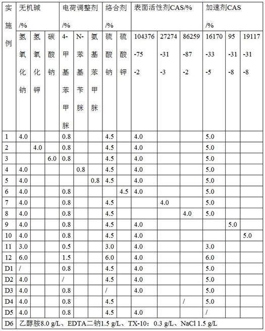
The invention discloses an oil-removing and hole-conditioning method of a printed circuit board PTH process, an alkaline oil-removing and hole-conditioning agent and a preparation method thereof, the oil-removing and hole-conditioning method of the printed circuit board PTH process comprises an alkaline oil-removing and hole-conditioning process, the alkaline oil-removing and hole-conditioning agent is used for treating a printed circuit board in the alkaline oil-removing and hole-conditioning process, and the alkaline oil-removing and hole-conditioning agent is used for treating the printed circuit board in the alkaline oil-removing and hole-conditioning process. The alkaline oil-removing pore-conditioning agent comprises a water solvent and the following components dissolved in the water solvent in percentage by mass: 3.0%-6.0% of inorganic alkali, 0.5%-1.5% of a charge regulator, 3.0%-6.0% of an inorganic salt complexing agent, 3.0%-6.0% of a nonionic surfactant and 3.0%-6.0% of an accelerator, the charge regulator is an amidine compound, and the accelerator is a sulfenamide compound. According to the method, the hole wall is subjected to hole finishing in the alkaline oil removal process, so that the hole wall has positive charges, adsorption of the hole wall to colloid palladium with negative charges is enhanced, and the hole wall copper plating quality is improved.
Description
technical field [0001] The invention relates to the technical field of printed circuit board manufacturing, and more particularly, to a method for removing oil and pore rectification in a PTH process of a printed circuit board, an alkaline degreaser and pore rectifying agent and a preparation method thereof. Background technique [0002] The PTH (hole metallization) process of the printed circuit board (PCB) is: the process of drilling the PCB board after going through the material cutting → inner layer dry film → browning → lamination process and depositing conductive metal on the inner wall of the through hole. The metallized vias are used to connect the circuit between the inner dry film and the outer dry film. [0003] With the development of high-density and high-definition circuit boards, the size of the interlayer connection metallized vias of multi-layer boards is getting smaller and smaller, and the PTH process is facing severe challenges. In the prior art, when th...
Claims
Login to View More Application Information
Patent Timeline
 IPC IPC(8): H05K3/00H05K3/42C23G1/20C23C18/18
CPCH05K3/002H05K3/42C23G1/20C23C18/1834
Inventor韦金宇李初荣
OwnerSHENZHEN BANMING SCI & TECH CO LTD